Self Bias or Potential Divider Bias Circuit:
This is the most commonly used biasing arrangement. The arrangement of Self Bias or Potential Divider Bias Circuit is shown in Fig. 12.17 (a). The name voltage divider is derived due to the fact that the voltage divider is formed by the resistors R1 and R2 across VCC. The emitter resistor RE provides stabilization. The resistor RE causes a voltage drop in a direction so as to reverse bias the emitter junction. Since the emitter-base junction is to be forward biased, the base voltage is obtained from supply VCC through R1 – R2 network.
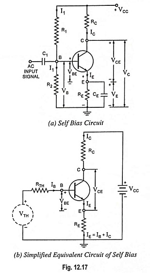
For forward biasing the emitter-base junction R1 and R2 are so adjusted that the base terminal becomes more positive than emitter. The net forward bias across the emitter-base junction, VBE is equal to VB minus dc voltage drop across RE. The dc bias circuit is independent of transistor current gain factor β. In case of amplifiers, to avoid the loss of ac signal (because of feedback caused by RE) a capacitor of large capacitance is connected across RE. The capacitor offers a very small reactance to the ac signal and so it passes through the capacitor.
Approximate Circuit Analysis:
Voltage divider bias circuits are usually designed to have the voltage divider current very much larger than the transistor base current IB and in this circumstance, base voltage VB is largely unaffected by base current IB and therefore, VB can be assumed to remain constant.
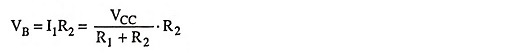
Assuming the current flowing through the resistor R1 to be equal to I1 and neglecting base current IB, being much smaller than voltage divider current, current flowing through resistance R2 can also be assumed to be equal to I1
![]()
Voltage across resistance R2,
Applying Kirchhoff’s second (or voltage) law to the base-emitter loop [Fig. 12.17(a)] we have
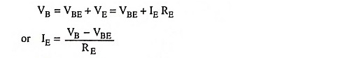
and collector current,

Applying Kirchhoff’s second (or voltage) law to the collector-emitter loop we have
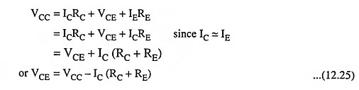
From Eqs. (12.24) and (12.25) the values of IC and VCE can be determined and the quiescent point Q is established.
It is clear from Eq. (12.24) that IC does not at all depend upon β. Though collector current lC depends upon VBE but in practice VBE is very small in comparison to VB and so collector current IC is practically independent of VBE. Thus collector current IC in this biasing circuit is almost independent of transistor parameters and hence good stabilization is ensured.
In this Potential Divider Bias Circuit the emitter resistance RE provides excellent stabilisation. This is explained as below :
Now let the temperature of transistor junction rise when it is loaded. This causes increase in leakage currents and so increase in the value of β. Hence collector current IC tends to increase. With the increase in the value of lC, voltage drop across emitter resistance RE increases. Since voltage drop across R2 (i.e. VB) is independent of collector current, therefore, VBE decreases and so IB, IE and Ic.
Thus we see that the Potential Divider Bias Circuit has tendency to hold the Q point (IC) stable automatically. This is due to feedback action. The increase in IC has immediately a reaction change of feedback so as to correct the situation.
Precise Circuit Analysis:
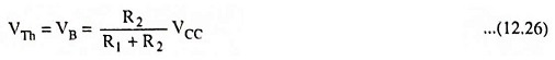
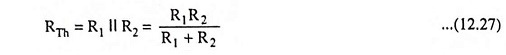
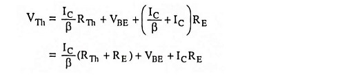
For exact analysis of a self bias or Potential Divider Bias Circuit, the voltage divider (the circuit to the left of the base terminal) is replaced by its Thevenin’s equivalent circuit, as shown in Fig. 12.17 (b).
Open-circuit voltage across base and ground terminals,
Resistance seen into the base and ground terminals with VCC short circuited,
Applying Kirchhoff’s voltage law around the closed base circuit [Fig. 12.17 (b)] yields
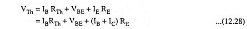
or Base current,
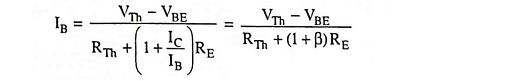
Once the base current has been determined, lC can be computed using appropriate value of β, and the transistor terminal voltages can then be computed.
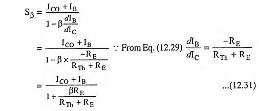
Stability Factor:
Differentiating Eq. (12.28) w.r.t. IC (considering VBE to be independent of lC) we have
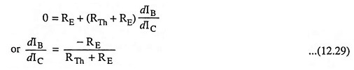
From Eq. (12.5) stability factor S is given as
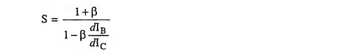
Substituting the value of dIB/dIC from Eq. (12.29) in above equation we have
Stability factor,
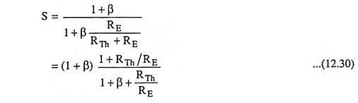
The above equation shows that stability factor S varies between 1 for small values of RTh/RE and (1 + β) for larger values of RTh/RE. For proper operation both RE and VCC should be larger and RTh small. Typical practical value of S for this type of biasing circuit is about 10.
Equation (12.28) may be written as
Differentiating above equation w.r.t. VBE, we have