Voltage Divider Bias Circuit:
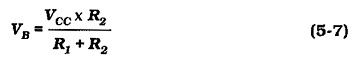
Circuit Operation – Voltage Divider Bias Circuit, also known as emitter current bias, is the most stable of the three basic transistor bias circuits. A voltage divider bias circuit is shown in Fig. 5-22(a), and the current and voltage conditions throughout the circuit are illustrated in Fig. 5-22(b). It is seen that, as well as the collector resistor (RC), there is an emitter resistor (RE) connected in series with the transistor. As discussed already, the total dc load in series with the transistor is (RC + RE), and this total resistance must be used when drawing the dc load line for the circuit. Resistors R1 and R2 constitute a voltage divider that divides the supply voltage to produce the base bias voltage (VB).
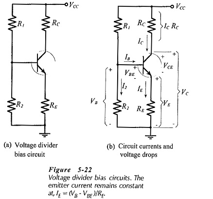
Voltage Divider Bias Circuit are normally designed to have the voltage divider current (I2) very much larger than the transistor base current (IB). In this circumstance, VB is largely unaffected by IB, so VB can be assumed to remain constant.
Referring to Fig. 5-22(b),
With VB constant, the voltage across the emitter resistor is also a constant quantity,![]()
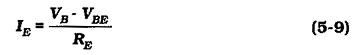
This means that the emitter current is constant,
The collector current is approximately equal to the emitter current, so IC is held at a constant level.
Again referring to Fig. 5-22(b), the transistor collector voltage is,
![]()
The collector-emitter voltage is,
![]()
VCE can also be determined as,
![]()
Clearly, with IC and IB constant, the transistor collector-emitter voltage remains at a constant level.
It should be noted that the transistor hFE value is not involved in any of the above equations.
Precise Circuit Analysis:
To precisely analyse a Voltage Divider Bias Circuit, the voltage divider must be replaced with its Thevenin equivalent circuit (VT in series with RT) as illustrated in Fig. 5-25. From Figure 5-25(a),
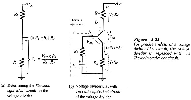
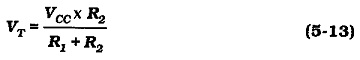
and RT is calculated as R1 in parallel with R2,
![]()
Referring to Fig. 5-25(b), an equation may be written for the voltage drops around the base-emitter circuit;
![]()
Substituting IC = hFE IB,
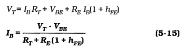
Once IB has been determined, IC can be calculated using the appropriate hFE value, and the transistor terminal voltages can then be calculated. The effects of the maximum and minimum hFE values can also be investigated.
Voltage Divider Circuit using Transistor:
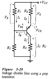
Voltage Divider Circuit using Transistor is shown in Fig. 5-29. Note that the positions of the collector and emitter resistors are reversed compared to the npn transistor circuit. Also, note that the base voltage (VB) in Fig. 5-29 is the voltage drop across resistor R1, not that across R2. As in the case of other circuits using pnp transistors, the current directions and voltage polarities are the reverse of those in npn transistor circuits. Apart from these differences, a pnp transistor Voltage Divider Bias Circuit is analysed in exactly the same way as an npn transistor circuit.