Base Bias Circuit With Collector and Emitter Feedback:
In this Base Bias Circuit With Collector and Emitter Feedback circuit, as obvious from its name, both collector and emitter feedbacks are used in an attempt to reduce circuit sensitivity to changes in β. Increase in β causes increase in emitter voltage but decreases collector voltage. As a result voltage across base resistor RB is reduced causing IB to fall thereby partially compensating the increase in β.
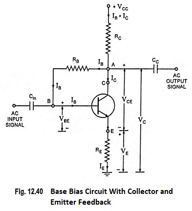
In this Base Bias Circuit With Collector and Emitter Feedback circuit a current flows in resistance RC from the supply VCC. At point A this current divides itself in two parts, one flowing in the collector of transistor, lC and the second part flows in the base resistor RB, IB. Thus current flowing in resistor RC will be equal to IB + IC.
No current flows to the output terminals since coupling capacitor CC offers infinite impedance to it (open circuit for dc).
Let the potential of point A be VC.
Applying Kirchhoff’s second law from point A to ground via RB, we have
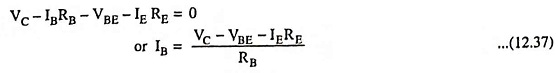
Neglecting VBE in comparison to collector potential VC which is usually very small.
![]()
Now applying Kirchhoff’s second law for circuit starting from VCC through collector to emitter terminal, we have

neglecting IB being too small and IE being almost equal to lC.
Applying Kirchhoff’s second law to the circuit starting from collector point A to E via RB
![]()
Comparing Eqs. (12.39) and (12.40) we have
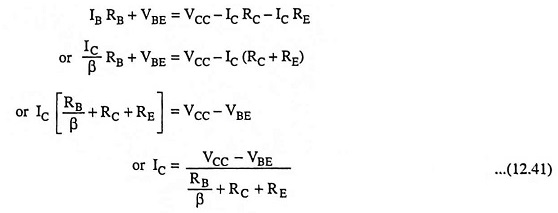
Neglecting VBE, being very small in comparison to supply voltage VCC,

The quiescent point, Q is thus established.
The circuit also stabilizes itself. Let the temperature of transistor junction rise when it is loaded. The increase in temperature causes increase in IC and β. When lC increases voltage drop in collector resistance RC i.e. lC RC increases and potential of collector drops. This causes reduction in value of base current IB which in turn reduces IC being equal to βIB.
Stability factor S:
Applying KVL to the input side, we have

Differentiating above equation w.r.t. lC we have

Substituting this value in general expression for S, we have