Voltage Divider Bias Circuit:
For the self-bias circuit, it was seen that increasing the resistance of RS brings ID(max) and ID(min) closer together, but that increased RS values result in lower ID levels. As will be demonstrated, Voltage Divider Bias Circuit allows RS to be increased without making ID very small.
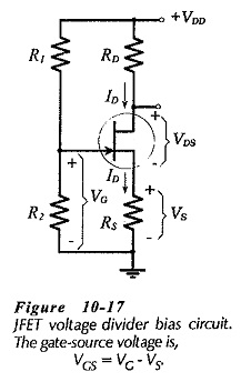
Figure 10-17 shows that a voltage divider bias circuit combines the use of a source resistor (RS) with a gate bias voltage (VG). The gate bias voltage is derived from the supply voltage by means of the voltage divider (R1 and R2), and the source voltage (VS) depends upon RS and ID. The gate terminal and the source terminal are both positive with respect to ground, and the gate-source voltage (VGS) is the difference between VG and VS. Because VS is larger than VG, the FET source terminal is at a higher level than the gate. So, the gate is negative with respect to the source, and the gate-channel junctions are reverse biased.
As in the case of a self-biased circuit, the voltage drop across RS increases if ID increases. This produces an increase in -VGS, which drives ID back toward its original level. A decrease in ID causes a reduction in -VGS which tends to increase ID.
Circuit Analysis:
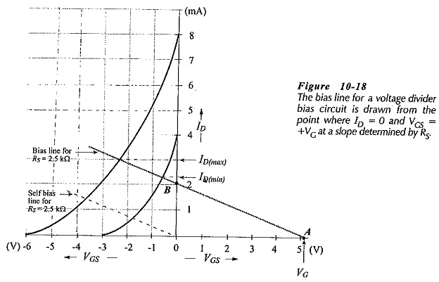
Once again, the graphical technique of drawing a bias line on the FET transfer characteristics is most convenient for analyzing a voltage divider bias circuit. An equation relating VGS and ID must be derived, so that corresponding values of each quantity may be calculated for plotting the bias line.
As discussed,
![]()
Because there is no gate current,
Referring to Eq. 10-6, it is seen that
![]()
This is a positive quantity, so the bias line is drawn from +VG, as shown in Fig. 10-18. It is seen that this gives higher drain current levels than those obtained when the bias line is drawn from ID = 0 and VGS = 0, (dashed line in Fig. 10-18).
Voltage Divider Bias for a p-channel JFET:
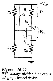
A voltage divider bias circuit using a p-channel JFET is shown in Fig. 10-22. As for the n-channel circuit, the gate-source bias voltage is the difference between VG and VS. In this case, these are both negative with respect to the positive supply voltage (VDD). Because VS is larger than VG, the gate terminal is positive with respect to the source, and this reverse biases the gate-channel junctions. A p-channel voltage divider bias circuit is analyzed in exactly the same way as an n-channel circuit.