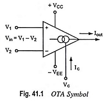
Operational Transconductance Amplifier (OTA):
The operational amplifiers considered up to this point have been voltage amplifiers. The input signal is a voltage and the output signal is a voltage. Another type of op-amp is an operational transconductance amplifier (OTA) which produces an output current proportional to an input voltage. The constant of proportionality is the transconductance of the amplifier. Thus, the OTA is voltage controlled current source (VCCS). There is usually an additional input for a current to control the amplifier’s transconductance. Ideally, the Operational Transconductance Amplifier has infinite input and output impedances, and the transconductance is assumed to be constant. However, real OTAs have noninfinite input and output impedances, and the transconductance is frequency dependent.
The IC OTAs are specially designed single chip transconductance amplifiers in which the input is voltage and the output is current such that
![]()
where gm is the transconductance or gain of the OTA. The unique feature of an Operational Transconductance Amplifier is that gm can be varied over a wide range by means of an external control current Ic. Usually, gm is proportional to Ic so that
![]()
where
![]()
The typical range of Ic is 0.1 μA to 1 mA.
Normally, OTAs are operated without feedback in linear applications. This is possible because the magnitude of the resistance attached to its output controls its output voltage. The major drawback is that if the differential input signal is not small, it may lead to distortion. Typically input signal remains below 100 mV peak-to-peak.
Operational Transconductance Amplifier finds applications in implementing programmable amplifiers and integrators in audio- processing and electronic music synthesis. They are also employed as current switches in sample and hold applications. One of the important use of OTAs using VLSI technique is in neutral networks. Popular OTAs are LM 3080, LMI 3600/3700 (National Semiconductor) CA 3080 (RCA) and the NE 5517 (Signetics).
The simplified internal circuit diagram of an OTA is shown in Fig. 41.2.
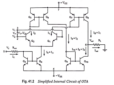
Transistor pairs Q1 – Q2 form a differential amplifier. Transistors Q3 – Q4 accept the controlling current Ic whose value is being controlled by an external resistor Rext and controlling voltage Vc. Since transistors Q3 – Q4 form current mirror,
![]()
Also, transistors Q5 – Q6 form current mirror, so that the current coming from collector of Q6 to Q9 duplicates I2.
So that,
![]()
Again transistors Q9 – Q10 form current mirror pair so that
![]()
The transistors Q7 – Q8 form current mirror pair and collector current of Q8 duplicates I1 so that
![]()
Now, at the output, applying Kirchoff’s current law, we have,
![]()
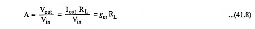
The voltage gain of the amplifier can be expressed as
The transconductance gm can be calculated as [behaving like diode]
![]()
where
Is = Reverse saturation current of transistor Q1 or transistor Q2 (assuming same characteristics)
and VT = Volt equivalent of temperature
![]()
Now the controlling current is given as
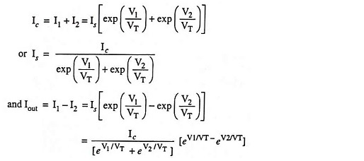
Multiplying numerator and denominator by exp
![]()
we have,
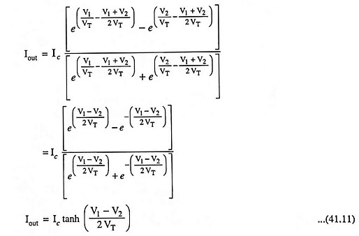
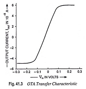
The above equation depicts that output current Iout is a function of differential voltage Vin i.e., (V1 – V2). Thus a transconductance amplifier normally computes a tan-hyperbolic. For smaller range of inputs the output current behaves linearly and smoothly shifts to saturation. Transfer characteristic of OTA is given in Fig. 41.3.
Equation (41.11) can be assumed as
![]()
Transconductance,
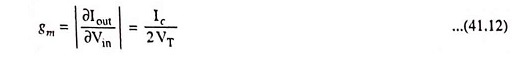
The voltage gain,
![]()
Thus, the voltage gain of the Operational Transconductance Amplifier is controlled externally by a controlling current Ic.
The OTA IC CA 3080 has few limitations as follows:
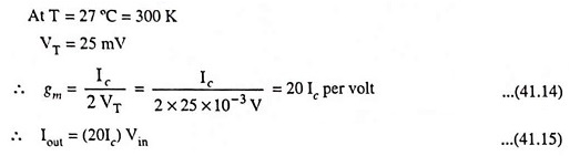
- It behaves linearly only when Iout < 400 μA and vin < 20 mV. Thus input voltage is limited to 20 mV only. (See Eq. 41.15).
- The inputs are fed directly to bases of transistors (Q2 and Q1) whose impedances are of the order of 10 kΩ to 30 kΩ. Therefore, loading effects may also occur when input signals are applied directly. Hence, op-amp voltage followers should be used to avoid loading effects.
Principal Differences From Standard Op-Amps: There are two main differences between the OTA and the conventional Op-amp:
- An Operational Transconductance Amplifier is a voltage controlled current source whereas the conventional op-amp is a voltage controlled voltage source (VCVS). OTA, being a current source, has a very high output impedance, in contrast to the op-amp’s very low output impedance. It is very well known that the low output impedance is a desirable feature in general amplifiers used to drive resistive loads.
- Another difference between OTAs and op-amps is that it is possible to design circuits using the OTA without using negative feedback. Thus, instead of using feedback for reducing the sensitivity of a circuits performance to device parameter, the transconductance gm is treated as a design parameter in place of resistors and capacitors in op-amps based circuits.