Photoconductivity – Definition, Working and its Applications:
Photoconductivity – When excess electrons and holes are produced in a semiconductor, there is a corresponding increase in conductivity of a sample as indicated by the following equation
Conductivity of semiconductor,
![]()
The above equation is obtained from Eqs. (6.48) and (6.59).
When the excess carriers in a semiconductor are due to optical luminescence, the resulting conductivity is called photoconductivity. This is an important effect, with useful applications in the analysis of semiconductor materials and in the operation of different types of devices.
The photoconductive effect is explained as follows:
The conductivity of a material is proportional to the concentration of charge carriers present, as indicated by Eq. (25.10). Radiant energy supplied to the semiconductor causes covalent bonds to the broken, and EHPs in excess of those generated thermally are produced. These increased current carriers reduce the resistance of the material and, therefore, such a device is called a photoconductor or photoresistor.
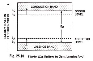
Energy diagram of a semiconductor having both acceptor and donor impurities is given in Fig. 25.10. When this specimen is illuminated by photons of sufficient energies, the possible transitions are as follows :
An EHP can be generated by a high-energy photon, in what is called intrinsic excitation; a photon may excite a donor electron into the conduction band ; or a valence electron may move into an acceptor state. The last two transitions are called the impurity excitations. Since the density of states in the conduction and valence bands greatly exceeds the density of impurity states, photoconductivity is due principally to intrinsic excitation.
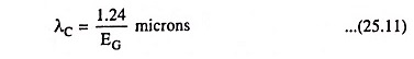
Spectral Response: The minimum energy of a photon required for intrinsic excitation is the forbidden-gap energy EG, in electron volts, of the semiconductor material. The long-wavelength threshold of the material is defined as the wavelength corresponding to the energy gap EG and is given by Eq. (25.11)
For silicon, EG = 1.1 eV and λC = 1.13 microns
whereas for germanium, EG = 0.72 eV and λC = 1.73 microns at room temperature.
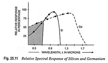
The spectral-sensitivity curves for silicon and germanium are given in Fig. 25.11. The worth noting point is that the long-wavelength limit is slightly greater than the calculated values of λC. This is due to impurity excitations. With the decrease of the wavelength, the response increases and attains a maximum value.
Photoconductive Current: The carriers generated by photoexcitation will move under the influence of an applied field, If they survive recombination, they will reach ohmic contacts at the ends of the semiconductor bar, and thus the device current will be constituted. The current may be given by
![]()
where GL is the generation rate of excess carriers, in cm-3 s-1, produced by optical luminescence, τ is the average life time of the newly generated carriers and tt is the average transit time for carriers to reach the ohmic contacts.
Photoconductor:
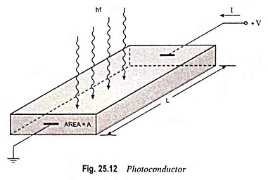
Figure 25.12 depicts a semiconductor bar with ohmic contacts at each end and a voltage applied between the terminals. The initial thermal-equilibrium conductivity is given by
![]()
When the excess carriers are created in the semiconductor, the conductivity becomes
![]()
where δn and δp are the excess electron and hole concentrations, respectively. Considering an N-type semiconductor, it can be assumed that δn = δp. Using δp as the concentration of excess carriers, in steady-state, the carrier concentration is given by
![]()
where GL is the generation rate of excess carriers and τh is the lifetime of excess minority carriers.
The conductivity from Eq. (25.14) can be written as
![]()
The change in conductivity due to the optical excitation, called a photoconductivity, is then
![]()
Applied voltage induces an electric field in the semiconductor and a current is caused by this electric field. The current density is given by
![]()
where J0 is the current density in the semiconductor prior to optical excitation and JL is the photocurrent density. The photocurrent density, JL = ΔσE. In case of uniform generation of excess electrons and holes throughout the semiconductor, photocurrent is given as
![]()
where A is the x-sectional area of the semiconductor device. The photocurrent varies directly as the excess carrier generation rate, which in turn is proportional to the incident photo flux.
If excess carriers (electrons and holes) are not generated uniformly throughout the semiconductor material, then the total photocurrent is determined by integrating the photoconductivity over the cross-sectional area.
Since μeE is the electron drift velocity, the electron transit time (time required for an electron to flow through the photoconductor) is given as
where L is the length of the semiconductor device.
The photocurrent is given, by Eq. (25.18),
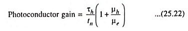
Photoconductor gain can be defined as the ratio of the rate at which charge is collected by the contacts to the rate at which charge is created within the photoconductor i.e.
and substituting the value of IL from Eq. (25.20) in Eq. (25.21) we have