Class A Power Amplifiers (Direct Coupled with Resistive Load):
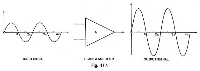
A class A power amplifiers is defined as a power amplifier in which output current flows for the entire cycle (360°) of the input signal, as illustrated in Fig. 17.4. In other words, the transistor remains forward biased throughout the input cycle.
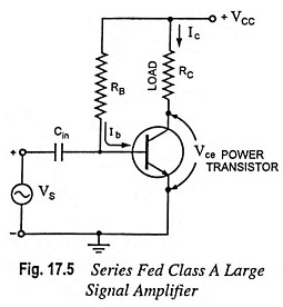
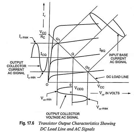
A schematic circuit of a series fed class A large signal amplifier using resistive load RC is shown in Fig. 17.5. The term “series fed” is derived from the fact that the load RC is connected in series with the transistor output. The only difference between this circuit and the small signal amplifier circuits considered previously is that the signals handled by the large signal circuit are in the range of volts and the transistor used is a power transistor capable of operating in the range of few watts. This circuit is seldom used for power amplification because of its poor collector efficiency but will provide clear understanding of class A operation to the readers. The output characteristics with operating point Q are shown in Fig. 17.6. ICQ and VCEQ represent no signal collector current and collector-emitter voltage respectively.
When an input ac signal is applied to the amplifier given in Fig. 17.5, the output will vary from its dc bias operating voltage and current. A small input signal, as indicated in Fig. 17.6. will cause the base current to vary above and below the dc bias point, which will then cause the collector current (output) Ic to vary from the dc bias point set as well as the collector-emitter voltage Vce to vary around its dc bias value. With the strengthening of the input signal, the output will vary further around the established dc bias point until either the current or voltage attains a limiting condition. For the current this limiting condition is either zero current at the lower end or VCC/RC at the upper end. For the collector-emitter voltage this limit is either 0 V or the supply voltage VCC. Let the output current vary between limits Ic min and Ic max and similarly the collector-emitter voltage between limits Vce min and Vce max.
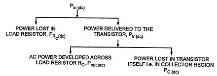
Power Distribution:
Input power from the collector supply VCC,
![]()
The power drawn from the collector supply is used in the following two components
(i) Power dissipated in collector load as heat,
![]()
(ii) Power supplied to the transistor,
![]()
Power supplied to the transistor, Ptr (dc) is further subdivided into
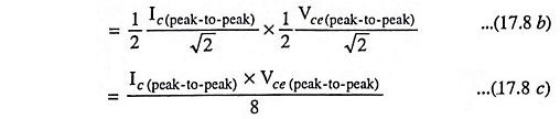
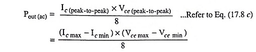
(a) ac power developed across the load resistor constituting ac power output and is given as
![]()
where Ic and Vce are the rms values of collector current and collector-emitter voltage
(b) Power dissipated, in the form of heat, by the transistor itself. The cause of power dissipation in transistor is explained below :
Consider an N-P-N transistor: The potential difference across the depletion layer formed near the collector junction is called the barrier potential. This potential provides the P-region (base) slightly more energy than N-region (collector). Thus when electrons emitted from emitter cross the base junction and enter the collector region, they give up energy in the form of heat and it is this energy that the transistor has to dissipate to the surrounding.
With zero signal applied at the input of the class A power amplifiers, ac power developed across the load reduces to zero and therefore, all the power fed to the transistor is wasted in the form of heat. Thus, a transistor dissipates maximum power under zero signal condition. Thus the device is cooler when delivering power to a load than with zero signal condition.
Since in class A operation, maximum power dissipation in the transistor occurs under zero signal condition, the power dissipation capacity of a power transistor, for class A operation, must be at least equal to the zero signal rating.
Power flow diagram of a transistor is given below :
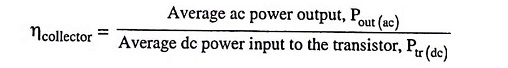
Collector Efficiency:
The collector efficiency of a transistor is given as
Power Efficiency:
A measure of the ability of an active device to convert the dc power of supply into the ac (signal) power delivered to the load is called the power or conversion or theoretical efficiency. By definition the efficiency is

Now ac power delivered to the load,
and from Eq. (17.5), total power drawn from dc supply,
![]()
So power efficiency,

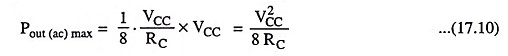
Maximum Power and Efficiency:
If the operating point Q is set at the midpoint of the maximum signal swing, the resulting maximum power condition may be achieved.
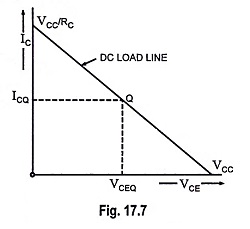
For the circuit shown in Fig. 17.7, this would be determined using

From Eq. (17.8 c) we have maximum ac power developed across the load resistor,
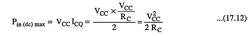
For the quiescent point Q,
![]()
and dc power drawn from dc supply,
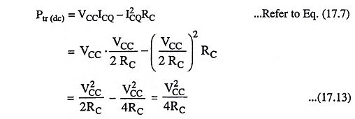
Power supplied to the transistor,
So maximum efficiency of an amplifier (class A power) is given as
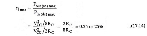
This is the maximum per cent efficiency for a series-fed class A power amplifiers. Since this maximum efficiency will occur only under ideal conditions and for the maximum ac signal swings, most series-fed class A power amplifiers have power efficiencies much less than 25%.
From Eqs. (17.10) and (17.13), we have
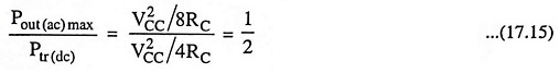
Thus, we see that a class A power amplifiers with a direct coupled resistive load can supply only one-half the amount of ac power to the load that the transistor can dissipate and the dc power input is four times the amount of ac signal power in the load.
Class A power amplifiers have got advantages of simple construction and distortion less output voltage.
The drawbacks of class A power amplifiers are very low efficiency and large power dissipation in the power transistors.