Direct Coupled Circuits:
For economy, the number of components used in any circuit should be kept to a minimum. The use of direct coupling between stages is one way of eliminating components. Figure 12-20 shows a Direct Coupled Circuits that has the base of transistor Q2 directly coupled to the collector of Q1.
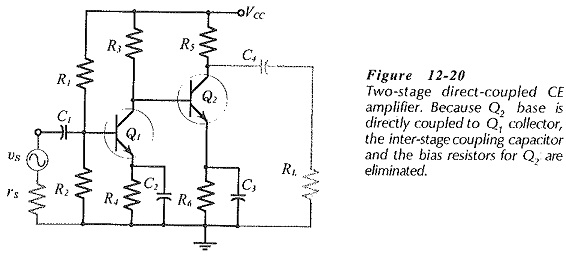
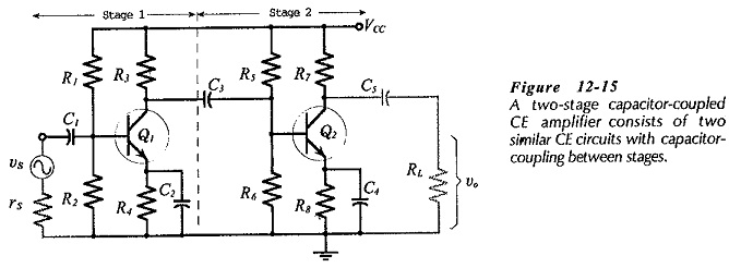
Comparing this to the capacitor-coupled circuit in Fig. 12-15, it is seen that the two bias resistors for Stage 2 and the interstage coupling capacitor have been eliminated. This is a saving of only three components, however, the total savings can be considerable when many similar circuits are to be manufactured.
Circuit Design:
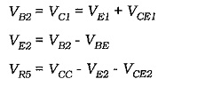
The first step in the design of the circuit in Fig. 12-20 involves determining a suitable level of base bias voltage for Q2. This is done by estimating satisfactory levels of VE1 and VCE1 for transistor Q1. Then,
As discussed already, appropriate dc voltage levels for small-signal amplifiers are VCE = 3 V and VE = 5 V, except in the case of a very low supply voltage.
As for all amplifier circuits, the resistor at the collector of the output transistor (R5 in Fig. 12-20) should be much smaller than the external load resistor. Once R5 is selected, IC2 can be calculated using the voltage VR5 already determined. If IC2 looks too small for satisfactory operation of the transistor, a suitable current level should be selected and a new value of R5 calculated. The collector current of Q1 is determined by making IC1, very much greater than the base current for Q2. This is done to ensure that IB2 has a negligible effect on the bias conditions of Q1. Normally, just making IC1 equal to IC2 is the simplest way to achieve the desired effect.
Circuit Analysis:
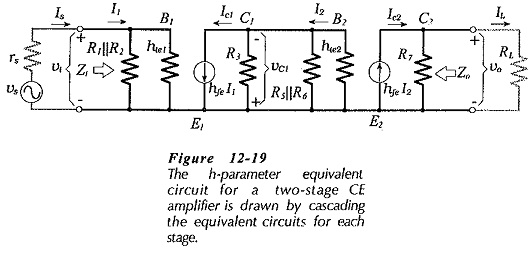
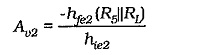
Analysis procedure for a two-stage Direct Coupled Circuits is similar to that for analysis of a two-stage capacitor-coupled circuit. The h-parameter equivalent for the circuit of Fig. 12-20 is exactly like Fig. 12-19, except that the bias resistors for the second stage are, omitted. The voltage gain and impedance equations are as determined for the capacitor-coupled circuit. Because the component numbers differ slightly for the two circuits, care must be taken in substituting components into the equations. For example, the voltage gain of the second stage of the circuit in Fig. 12-20 is,
Use of Complementary Transistors:
The Direct Coupled Circuits, two-stage circuit illustrated in Fig. 12-22 is similar to that in Fig. 12-20, except that transistor Q2 is a pnp device. The transistors are selected to have similar characteristics and parameters although one is npn and the other is pnp. This means that they are complementary transistors.
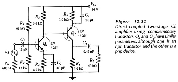
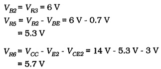
Suppose the circuit in Fig. 12-22 is to be designed to use a 14 V supply, as in Example 12-8. Allowing VE1 = 5 V and VCE1 = 3 V, the base voltage for Q2 (measured from +VCC) is,
The use of complementary transistors in Fig. 12-22 reduces the voltage drop across the emitter resistor of Q2, compared to the situation in Fig. 12-20. This makes more voltage available for dropping across the Q2 collector resistor.
The design procedure for the circuit using complementary transistors is very similar to the procedure for designing the non-complementary circuit in Fig. 12-20.