Transistor Detector Circuit Working Principle:
It is possible to achieve amplitude demodulation by using a three-element electronic device. A typical example of such a configuration is illustrated in Fig. 22.51. This circuit is called a transistor detector.
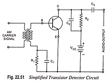
In addition to detection of the modulated carrier input signal, it also furnishes amplification of the modulating signal. It should be noted that when used as a detector, the transistor has to be biased at cutoff or operated as class B. For transistor detector circuit shown in Fig. 22.51 conduction occurs only from emitter to base because of the diode action associated with these elements.
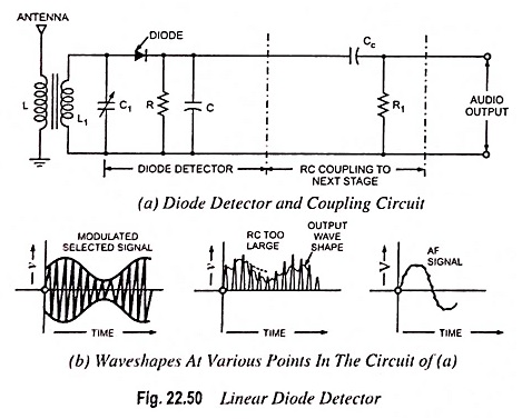
It can be easily seen that the AM wave is rectified in the emitter-base circuit in precisely the same manner as occurs in the diode detector shown in Fig. 22.50(a). In fact resistor R1 and capacitor C1 serve the same purpose as do R and C in Fig. 22.50(a).
The voltage developed across R1 in Fig. 22.51 varies in accordance with the modulating signal rate. Since this variation exists in the transistor input circuit, it causes a corresponding amplified variation to occur in the collector-circuit, specifically across R2. Capacitor C2 is selected to bypass the carrier frequency signal and C3 serves to block the dc voltage level from passing to the next stage. As a result, the voltage appearing across the output terminals of this circuit is an amplified version of the modulating portion of the input signal.