Foster Seeley Detector – Circuit Diagram, Working and its Phasor Diagram:
The circuit diagram of the Foster Seeley detector is shown in Fig. 22.54. This Foster Seeley Detector circuit consists of an inductively coupled double tuned circuit in which both primary and secondary coils are tuned to the same frequency (intermediate frequency).
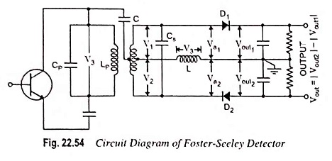
The centre of the secondary coil is connected to the top of the primary (collector end) through a capacitor C. This capacitor C performs the following functions:
- It blocks the dc from primary to secondary.
- It couples the signal frequency from primary to centre tapping of secondary.
The primary voltage V3 (i.e., the signal voltage) thus appears across the inductor L. Nearly entire voltage V3 appears across inductor L except a small drop across the capacitor C. However, by a suitable choice of C and L, the voltage drop across the capacitor C can be made negligible.
The centre tapping of the secondary coil has an equal and opposite voltage across each half winding. Hence V1 and V2 are equal in magnitude but opposite in phase. The radio frequency voltages Va1 and Va2 applied to the diodes D1 and D2 are expressed as
![]()
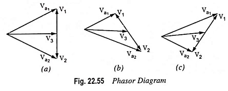
Voltage Va1 and Va2 depend upon the phase relations between V1, V2 and V3. The phasor diagrams of Foster Seeley Detector for different frequencies have been shown in Fig. 22.55. The phasors V1 and V2 are always equal in magnitude but in phase opposition. However, the phase position of V1 and V2 relative to V3 would depend upon the tuned secondary coil at the resonance or off the resonance as discussed below :
1. At Resonance: When an input voltage has a frequency equal to the resonant frequency fif of the tuned secondary, V3 is in phase quadrature (90° out of phase) with V1 and V2. This has been indicated in Fig. 22.55 (a). The resultant voltages Va1 and Va2 are equal in magnitude.
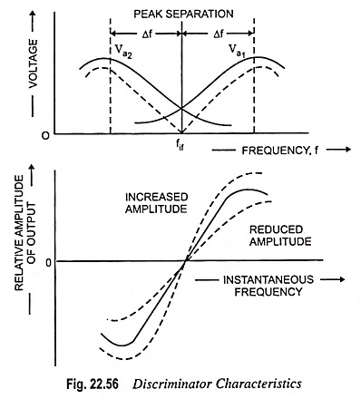
2. Off Resonance: When the input voltage is off the resonant frequency fif of the tuned secondary, the phase position of V1 and V2 relative to V3 will be different from 90°. Let Qs be the quality factor of tuned secondary coil. When an input signal frequency exceeds the resonant frequency fif by an amount fif/2Qs the phase difference between V3 and V1 is 45° as shown in Fig. 22.55 (b). Because V2 is in phase opposition of V1, the phase difference between V3 and V2 is 135°. The phasor diagram shown in Fig. 22.55 (b) reveals that Va1 is reduced whereas Va2 is increased. The situation is reversed when the input voltage has a frequency below fif which is evident from the phasor diagram shown in Fig. 22.55 (c). Thus the magnitude of the voltages Va1 and Va2 will vary with the instantaneous frequency f in the manner shown in Fig. 22.56.
The RF voltages Va1 and Va2 are separately rectified by the diodes D1 and D2 respectively to provide voltages Vout1 and Vout2. The RF components are bypassed by the capacitors leaving only modulating frequency component and a dc term. The voltages Vout1 and Vout2 then represent the amplitude variations of voltages Va1 and Va2 respectively. The diodes are so arranged that the output voltage Vout is equal to the arithmetic difference | Vout2 | – | Vout1 |.
![]()
Thus, the output voltage Vout will vary with instantaneous frequency in accordance with the difference | Vout2 | – | Vout1 |, as shown by the dotted curve in Fig. 22.56 (b). This allotted curve is known as discriminator characteristic in Fig. 22.56.