Early Effect and Base Width Modulation:
In active region, the emitter-base (EB) junction is forward biased and collector-base (CB) junction is reverse biased, so the barrier width at EB junction is negligible in comparison with the space-charge width at CB junction, as illustrated in Fig. 10.20.
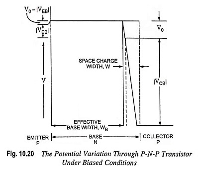
The transition or space-charge region at a junction is the region of uncovered charges on both sides of the junction. As the voltage applied across the junction increases, the transition region penetrates deeper into the collector and base. Because neutrality of the charge is to be maintained, the number of uncovered charges on each side remains equal. Since the doping in the base is substantially smaller than that of collector, the penetration of the transition region into the base is much larger than that into the collector region. Hence the collector depletion region is neglected and all the immobile charge is indicated in the base region.
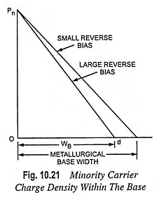
As obvious from Fig. 10.21 the effective base width is metallurgical base width less space charge width W. This modulation of the effective base width by the collector voltage VCB is known as the Early effect.
An increase in magnitude of collector voltage increases space-charge width W at the output junction diode and this, in turn, causes the effective base width WB to decrease.
The decrease in effective base width WB with increasing reverse bias has three consequences.
- There is less chance for recombination within the base region. Hence the transport factor β and also α, increase with an increase in the magnitude of CB junction voltage.
- The concentration gradient of minority carriers is increased within the base, and consequently, the current of minority carriers injected across the emitter junction increases, with increasing reverse collector voltage.
- For extremely large voltages, WB may be reduced to zero causing voltage breakdown. When effective base width WB is reduced to zero, the emitter barrier becomes V’, which is smaller than normal value V0 – |VEB| because the collector voltage has reached through the base region. This lowering of the emitter-junction voltage causes an excessively large emitter current, thus placing an upper limit on the magnitude of the collector voltage. This phenomenon is known as punch through.
The punch-through (or reach-through) phenomenon may be defined as the mechanism by which a transistor usefulness may be terminated by increasing the collector voltage.