Transistor Terminals (Emitter, Collector and Base):
As mentioned already, transistor is a single crystal in which there are two P-N junctions, as shown in Fig. 10.1. The idea behind is to have first section to supply the charges (either holes or electrons) to be collected by the third section through the middle section. One side section supplying free charges is called the emitter, other side section collecting these charges is called the collector and the middle section which is formed between the emitter and collector is called the base. The Three Transistor terminals are discussed below
1. Emitter – It is left hand section (or region) of the transistor and its main function is to supply majority charge carriers (electrons in case of NPN transistors and holes in case of P-N-P transistors) to the base. The emitter is always forward biased w.r.t. base so that it is able to supply majority charge carriers to the base. The emitter is heavily doped so that it may be able to inject a large number of charge carriers. It is of moderate size in order to maintain heavy doping without diluting it or mesh formation in it.
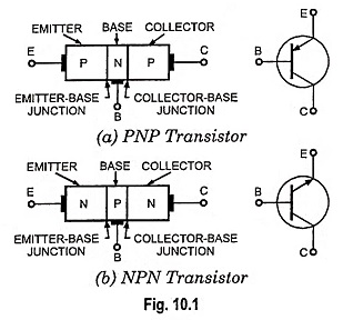
2. Collector – It is the right hand section of the transistor and its main function is to collect majority charge carriers. Collector is always reverse biased so as to remove the charge carriers away from its junction with the base. It is moderately doped to avoid the chances of mesh formation even after taking the carriers from the emitter. Large in size to withstand the temperature generated at the collector.
3. Base – It is the middle section of the transistor and is very lightly doped to reduce the recombination within the base so as to increase collector current and is very thin (of the order of μm) in comparison to either emitter or collector so that it may pass most of the injected charge carriers to the collector.
Base forms two junctions i.e., emitter junction and collector junction, each having its own barrier voltage. The forward-biased emitter-base junction offers low resistance to the emitter current whereas the collector-base junction, which is reverse biased, offers high resistance to the collector current. As the resistance of emitter-base junction is very small as compared to that of collector-base junction, therefore, the forward bias applied to the emitter-base junction is usually very small whereas the reverse bias on the collector-base junction is much large.
In most of the transistor terminals, the collector region is made physically larger than emitter region because collector is to dissipate much power. Due to this difference, collector and emitter are not interchangeable. However, for sake of convenience, it is customary to show emitter and collector to be of equal size.
As regards the symbols, arrowhead is always at the emitter. The direction indicates the conventional direction of current flow (from emitter to base in case of P-N-P transistor and from base to emitter in case of NPN transistor). Generally, no arrow head is marked for collector since its reverse leakage current is always opposite to the direction of emitter current.