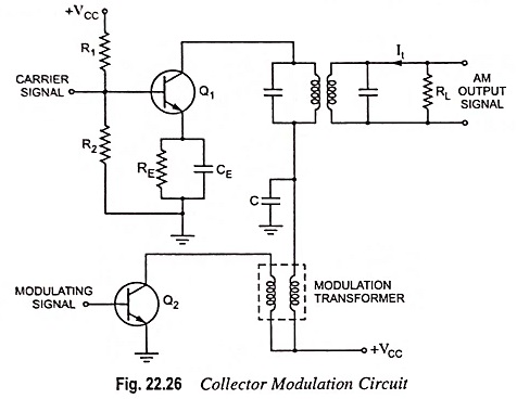
Collector Modulation Circuit – Working, Advantages and Disadvantages:
This is very popular method for AM generation. The circuit diagram for collector modulation is shown in Fig. 22.26. Here, the transistor Q1 makes an RF class C amplifier. The carrier signal is applied to the base of Q1. VCC makes collector supply used for biasing purpose. Also, the transistor Q2 makes a class B amplifier which is used to amplify the audio or modulating signal. The modulating or baseband signal appears across the modulation transformer after amplification. The amplified modulating signal appears in series with collector supply VCC. The function of capacitor C is to offer low impedance path to high frequency carrier signal and, therefore, the carrier signal is prevented from flowing through the modulation transformer.
Working Principle of Collector Modulation:
It is a known fact that in a class-C amplifier, the magnitude of output voltage is a definite fraction of or at the most equal to supply voltage VCC. In addition to this, a linear relationship exists between the output tank current It and the variable supply voltage Vc (here it has been assumed that supply voltage VCC is a varying quantity and its varying value is denoted by Vc). This means that in class C amplifier, the output voltage will be an exact replica of the input voltage waveform and the magnitude of output voltage will be approximately equal to carrier supply voltage VCC. Now if R is the resistance of the output tank circuit at resonance, then the magnitude of output voltage is given as
RIt ≡ VCC
So, the unmodulated carrier is amplified by class C modulation amplifier using transistor Q1 and its magnitude will remain constant at VCC since there appears no voltage across the modulation transformer in the absence of modulating signal.
But now if a modulating voltage vm = Vm cos ωmt appears across the modulation transformer, this signal will be added to the carrier supply voltage VCC. This results in a quite slow variation in carrier supply voltage VCC. This type of slow variation in carrier supply voltage changes the magnitude of the carrier signal voltage and the output of the modulated class C amplifier as shown in Fig. 22.27.
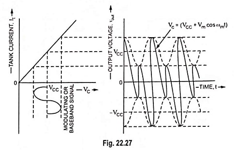
It may be observed that the envelope of the output voltage is identical with the modulating voltage and thus AM signal is produced.
Mathematical Analysis:
The slowly varying carrier supply voltage Vc may be expressed as
Let the carrier voltage be vC = VCC cos ωct
Then the modulated output voltage will be
![]()
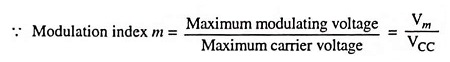
Substituting the value of Vc in above equation from Eq. (22.32), we have
![]()
which is required expression for AM wave.
Advantages:
- Good linearity.
- High collector circuit efficiency.
- High power output per transistor.
Disadvantages:
- Large modulating power requirement.
- Hundred per cent modulation cannot be achieved because of collector saturation.