N Channel Power MOSFETs or V-MOSFET or V-FET:
N Channel Power MOSFETs – Power MOSFETs are usually constructed in V-configuration, as shown in Fig. 13.94. That is why, the device is sometimes called the V-MOSFET or V-FET. V-shaped cut penetrates from the device surface almost to the N+ substrate through N+, P and N– layers, as seen from Fig. 13.94. The N+ layers are heavily doped, low resistive material, while the N– layer is a lightly doped, high-resistance region. The silicon dioxide dielectric layer covers both the horizontal surface and V-cut surface. The insulated gate is metal film deposited on the SiO2 in the V-cut. Source terminals make contact to the upper N+ and P-layers through the SiO2 layer. The N+ substrate is the drain terminal of the device.
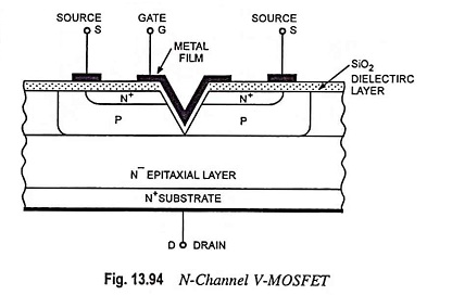
V-MOSFET is an E-mode FET and no channel exists between drain and source regions until the gate is made positive w.r.t. the source. On making gate positive w.r.t. the source, an N-type channel is formed close to the gate, as in the case of an E-MOSFET. In this case, N-type channel provides a vertical path for the charge carriers to flow between the N+ substrate (i.e., drain) and the N+ source termination. When VGS is zero or negative, no channel exists and the drain current is zero.
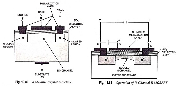
The drain and transfer characteristics for the enhancement-mode N Channel Power MOSFETs are similar to those for the EMOSFET, as illustrated in Figs. 13.80 and 13.81 respectively. With the increase in gate voltage, the channel resistance is reduced and, therefore, the drain current ID increases. Thus the drain current ID can be controlled by gate voltage control so that for a given level of VGS, ID remains fairly constant over a wide range of VDS levels.
Drain terminal being at the bottom of the V-MOSFET (instead of at the top surface) can have a considerable large area for any given size of the device. This allows much greater power dissipations than are possible in a MOSFET having both drain and source at the surface.
In the power or V-MOSFETs the channel length is determined by the diffusion process, while in other MOSFETs the channel length depends upon the dimensions of the photographic masks used in the diffusion process. By controlling the doping density and the diffusion time, much shorter channels can be produced than are possible with mask control of channel length. These shorter channels allow much more current densities, which again contribute to larger power dissipations. The shorter channel length also allows a larger transconductance gm to be attained in the V-FET and very considerably improves the frequency response and the device switching time.
Another very important factor in the geometry of the power MOSFET is the presence of the lightly doped N– epitaxial layer close to the N+ substrate. When VGS is zero or negative and the drain is positive w.r.t. the source, the junction between the Player and the N– layer is reverse biased. The depletion region at this junction penetrates deep into the N– layer and thus punch-through from drain to source are avoided. So relatively high VDS can be applied without any danger of device breakdown.
P-channel V-MOSFETs are also available. Their characteristics are similar to those of N-channel MOSFETs, except that the current directions and voltage polarities are reversed.
Advantages of N Channel Power MOSFETs:
One main advantage of power MOSFETs over BJTs is the lack of thermal runaway. The RDS(on) of a MOSFET has a positive temperature coefficient. With the increase in internal temperature, RDS(on) increases, and reduces the drain current ID which lowers the temperature. As a result, power MOSFETs are inherently temperature-stable and cannot go into thermal runaway.
Another advantage of N Channel Power MOSFETs is that they can be operated in parallel while power BJTs cannot, because in BJTs, VBE drops do not match closely enough. If the BJTs are connected in parallel, current hogging occurs. This means that the BJT with the lower VBE takes more collector current than the others. Power MOSFETs in parallel do not suffer from the problem of current hogging. If one of the power MOSFET tries to hog the current, its temperature will increase. This causes increase in its RDS(on), which reduces its drain current. The overall effect is for all the power MOSFETs to have equal drain currents.
In addition to above, N Channel Power MOSFETs have the advantage of switching a large current off faster than a BJT can, because a power MOSFET does not have minority carriers. Typically, a power MOSFET can switch off amperes of current in tens of nanoseconds. This is 10 to 100 times faster than with a comparable BJT.
Power MOSFET as an Interface:
Digital ICs are low-power devices and if they are to be used to drive a high-current load, power MOSFET can be used as an interface (a device B that allows device A to communicate with or control device C).
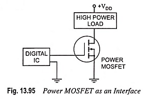
Figure 13.95 illustrates how a digital IC can control a high-power load. The output of the digital IC drives the gate of the power MOSFET. When the digital output is high, the power MOSFET acts like a closed switch. When the digital output is low, the power MOSFET acts like an open switch. Interfacing digital ICs to a high-power loads is one of the important application of power MOSFET.