FET Amplification:
Consider the n-channel FET Amplification circuit in Fig. 9-26. Note that drain-source terminals are provided with a dc supply (VDD), connected via the drain resistor (R1). The gate-source junctions are reverse-biased by the gate voltage (VG). An ac signal generator (with voltage vf) is connected in series with the gate terminal. As already discussed, field effect transistors are voltage-operated devices. The drain current is controlled by the gate-source voltage. A change in gate-source voltage (ΔVGS) produces a change in drain current (ΔID), and this causes a variation in the voltage drop across the resistor connected in series with the drain terminal.
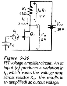
Suppose that, for the circuit in Fig. 9-26, VDD = 20 V, R1 = 6 kΩ, and VG is adjusted to give ID = 2 mA. Also, assume that the FET has a forward transfer admittance of Yfs = 4000 μS. The dc level of the drain voltage is,
![]()
Now assume that the instantaneous level of vi is +50 mV. This produces an increase,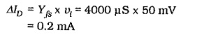
The new level of drain voltage is,
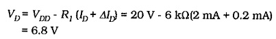
So, VD changed from 8 V to 6.8 V when the ac input increased from zero to 50 mV.
When the instantaneous level of vi is -50 mV,
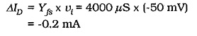
This gives a new drain voltage,
It is seen that an ac input of vi = ±50 mV produces an output voltage change at the FET drain terminal of ΔVD = ±1.2 V. This can be stated as an ac output voltage of vo = ±1.2 V.
The circuit voltage amplification is,