Frequency Response of FET Amplifier:
Low-Frequency Response – The low Frequency Response of FET Amplifier circuits is determined by exactly the same considerations as for BJT circuits. The lower cutoff frequency is normally set by a source bypass capacitor, and it can be affected by coupling capacitors.
High Frequency Response:
Unlike BJTs, a device cutoff frequency is not normally specified for a FET. Instead, FETs intended for high-frequency operation have the parameters listed as measured at a specified high frequency. The low-frequency parameters are also normally listed. For example, a 2N5484 JFET has the following parameters: 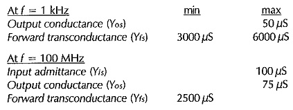
The device inter-terminal capacitances (Cgs, Cgd, and Cds) are important quantities in determining the performance of a FET circuit, and these are used in the same way as the BJT capacitances. An input capacitance limited cutoff frequency (f2(i)), and an output capacitance limited cutoff frequency (f2(o)) can be calculated. The input capacitance is amplified by the Miller effect in the case of a CS circuit (an inverting amplifier). Equation for the FET circuit,
![]()
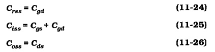
The FET capacitances are specified as the input capacitance (Ciss), the reverse transfer capacitance (Crss), and the output capacitance (Coss). The reverse transfer capacitance is another name for the gate-drain capacitance. The input capacitance is the sum of the gate-source capacitance and the gate-drain capacitance. The output capacitance is simply the drain-source capacitance.
Typical input capacitance values for a 2N5484 high-frequency JFET are: Crss = 1 pF, Ciss = 5 pF, Coss = 2 pF. Because, these are extremely small, the circuit performance can be easily affected by stray capacitance.