Transistor as a Switch Circuit Diagram and Working:
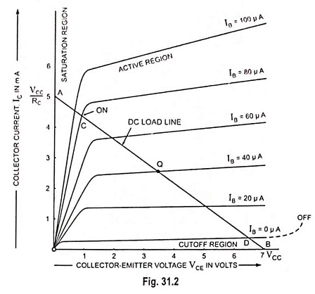
The Transistor as a Switch Circuit Diagram and Working can be explained with the help of its output characteristics. Figure 31.2 shows the output characteristics of a typical transistor for a CE configuration. The dc load line for a given collector supply voltage VCC and collector resistance RC is drawn on the output characteristics. The three regions viz. cutoff region, active region and saturation region are clearly marked on the output characteristics.
When the base input voltage polarity is such that the transistor is biased off (base current IB is zero), as shown in Fig. 31.1 (a). the only current flowing through the collector will be the collector leakage current ICEO. As a result there is little voltage drop across collector resistor RC and as such output voltage (collector-emitter voltage VCE) becomes almost equal to VCC. Under this condition the transistor operates at cutoff. This is off state of the transistor switch.
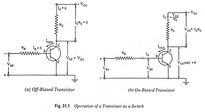
On the other hand, when the base-emitter junction is forward biased to the extent that the transistor is saturated, maximum possible collector current, called the saturation current lC (sat), flows through the collector resistance RC (corresponding to point C in Fig. 31.2) making voltage drop across it almost equal to VCC. Under this operating condition shown in Fig. 31.1 (b), the output voltage (voltage across collector-emitter terminals) VCE is almost zero (less than 1 V) and the collector emitter terminals behave as closed contacts for the main collector current.
When a transistor is working as a switch, the cutoff (off) and saturation (on) regions are the stable regions of its operation, while active region is the unstable (or transient) region of its operation. The operation of transistor passes through the active region when its condition is changed from one state to another (i.e., from off state to on state or vice versa). In Fig. 31.2 the DC is the active region. The collector current lC increases from ICEO to lC (sat) along the path DC as the transistor is switched On. When the transistor is switched off, IC decreases from lC (sat) to ICEO along path CD.
In the ‘off state’ of a transistor switch, as discussed above, the collector current is not absolutely zero but some leakage current (current due to minority carriers) does flow and as such the resistance between its collector-emitter terminals is not infinite, though it is very high. Similarly in the ‘on state’ of a transistor switch the voltage across its collector-emitter terminals is not zero, though it is very small (less than 1 V) and as such the resistance between its collector-emitter terminals is not absolutely zero. Thus the transistor does not behave as an ideal switch, but in other respects it is superior to switches of other types, particularly from the point of view of operating speed. For high speed switching, transistor is the only device.
The electronic switches can be employed for generating nonsinusoidal waves such as square, rectangular and sawtooth waves.
Proper design for switching operation requires that the operating point switches from cutoff to saturation along the load line, as shown in Fig. 31.3. For our purposes we will assume the IC = ICEO = 0 mA when IB = 0μA as shown in Fig. 31.3 (an excellent approximation in the light of improving fabrication techniques). In addition we will assume that VCE = VCE (sat) = 0 V rather than the typical 0.1 to 0.3 V level.
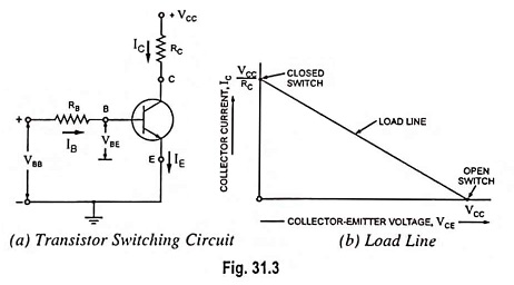
Transistor switching circuit is shown in Fig. 31.3 (a). Summing up voltages around the input loop provides
![]()
or Base current,
![]()
For a silicon transistor VBE is typically 0.7 V.
If the base current is larger than or equal to IB (sat), the operating point Q is at the upper end of the load line [Fig. 31.3 (b)]. In this case, the transistor appears like a closed switch. On the other hand, if the base current is zero, the transistor operates at the lower end of the load line and the transistor appears like an open switch.
In Fig. 31.4 we see a transistor switching circuit that is being driven by a voltage step. This is the kind of waveform we get in a digital computer. When the input voltage is zero, the transistor is cutoff, it appears like an open switch. With no current through the collector resistor, the output voltage equals VCC (+10 V).
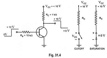
When the input voltage is 10 V, the base current is
![]()
Visualizing the transistor shorted between the collector and emitter, the output voltage ideally drops to zero, and the saturation current is
![]()
If the hfe of the transistor is 100 and IB = 0.93 mA, the collector current will attempt to be IC = hfe IB = 100 x 0.93 mA = 93 mA.
Obviously the collector current can never attain this value as it is limited by the collector resistance RC of 1 kΩ. The conclusion to be drawn is that when input voltage is 10 V, the collector current will be the maximum and equal to saturation current IC (sat) and VCE will be approximately zero.
Thus, we see that when input voltage is zero, output voltage VCE is maximum and equals VCC and when input voltage is maximum, the output voltage VCE is minimum and is almost zero. It means output is inverse of the input and the transistor switch acts like an inverter.
The power loss in the on-state is quite low because VCE (sat) is very small and power loss is given as
![]()
Thus the transistor efficiency is quite high in on-state.
The power loss in the off-state equals collector supply voltage multiplied by reverse leakage current ICEO. Since ICEO is negligibly small as compared to full-load current that flows in the on-state, power loss in the transistor is quite small in the qff-state. Thus the efficiency of the transistor is high in off-state too.
Fixed Current Bias Transistor Switching Circuit:
The fixed current bias circuit for transistor switching is shown in Fig. 31.5. In this case, the transistor is biased into saturation. Unlike amplifier circuits, the bias conditions of properly designed switching circuits do not normally change with different transistor hfe values. The switching transistor is either on or off. Although too unpredictable for biasing amplifier circuits, fixed current bias is quite satisfactory for switching circuits.
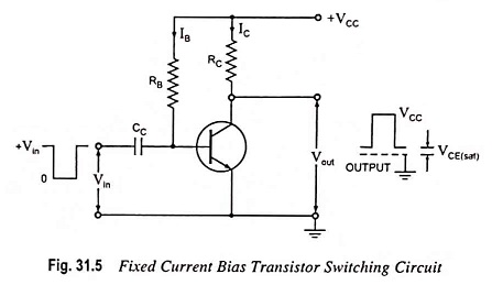
For the circuit shown in Fig. 31.5, base current IB is determined using the specified minimum value of hfe and collector current IC level required for saturation. Base resistance RB is then determined from the collector supply voltage VCC and base current IB levels. This means that all hfe values higher than hfe (min) will give collector currents larger than that required for saturation. Thus, the transistor is always saturated regardless of the value of hfe.
The negative-going input pulse, applied to the transistor base via capacitor CC, drives the base below the emitter voltage level to switch the device off. When the transistor goes off, collector current IC ceases to flow and output voltage Vout goes from VCE (sat) to approximately VCC.