FET as a Voltage Variable Resistor (VVR):
FET is a device that is usually operated in the constant-current portion of its output characteristics. But if it is operated in the region prior to pinch-off (i.e., where VDS is small, say below 100 mV), it will behave as a Voltage Variable Resistor (VVR). It is due to the fact that in this region drain-to-source resistance RDS can be controlled by varying the gate bias voltage VGS. In such applications the FET as a Voltage Variable Resistor (VVR) or voltage dependent resistor.
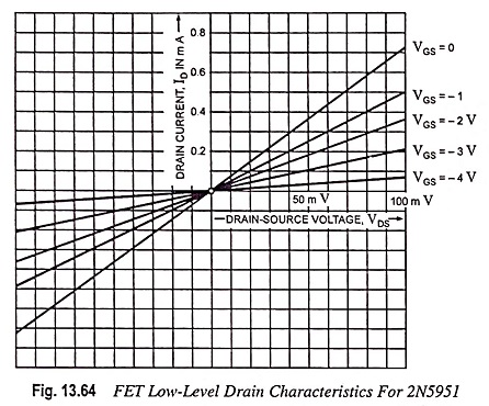
Figure 13.64 shows the drain characteristic curves for a 2N5951 in the ohmic region (i.e., for low VDS). From the characteristic curve it can be seen that RDS varies with VGS. For example, when VGS = 0, RDS = 133 Ω and when VGS = – 2 V, RDS = 250 Ω. Because of this a JFET operating in the ohmic region with small ac signals acts as a voltage-controlled resistance.
Note that the drain curves shown in Fig. 13.64 extend on both sides of the origin. This means that a FET as a Voltage Variable Resistor (VVR) for small ac signals, typically those less than 100 mV. When it is employed in this way, it does not require a dc drain voltage from the supply. All that is required is an ac input signal.
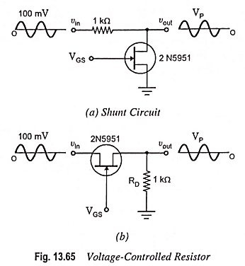
Figure 13.65 (a) shows a shunt circuit where the FET as a Voltage Variable Resistor (VVR). This circuit is identical to the JFET shunt switch discussed earlier. The difference is that the gate bias voltage (control voltage) VGS does not swing from 0 to a large negative value. Instead, VGS can vary continuously i.e., it can have any value between 0 and VGS (off). Thus, VGS controls the resistance of the JFET, which then changes the peak output voltage.
Figure 13.65 (b) depicts a series circuit with the FET as a Voltage Variable Resistor (VVR). The basic idea is the same. By varying VGS, the ac resistance of the JFET can be varied, which causes variation in the peak output voltage, VP.
Application of VVR in Automatic Gain Control:
Since the FET operated, as described above, behaves like a variable resistor, it finds applications in many areas where this property is useful. The VVR, for example, can be employed for varying the voltage gain of a multistage amplifier as the signal level varies.
When a receiver is tuned from a weak to a strong station, the loudspeaker will blare (become loud) unless the volume is immediately reduced. The volume may also change because of fading, a decrease in signal caused by a change in the path between the transmitter and receiver. To avoid undesirable variations in the volume, automatic gain control (AGC) is used in most modern receivers.
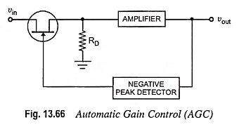
The basic idea of AGC is depicted in Fig. 13.66. An input signal vin is passed through a JFET employed as a VVR. The signal is amplified to get the output voltage vout. The output signal is fed back to a negative peak detector. The output of this peak detector supplies the gate bias voltage VGS for the JFET.
In case the input signal gets strengthened by a considerable amount, the output voltage will increase. It means that a large negative voltage comes out of peak detector. Since VGS becomes more negative, the JFET has a higher ohmic resistance, which reduces the strength of the signal supplied to the amplifier and thus output signal is reduced.
On the other hand, if the input signal becomes weaker, the output voltage falls and the negative peak detector gives a smaller output. Since VGS becomes lesser negative, the JFET transmits stronger signal to the amplifier, which raises the output. Thus the effect of any sudden change in the input signal is offset or at least reduced by the AGC action.