What is Intrinsic Semiconductor?
An intrinsic semiconductor is one which is made of the semiconductor material in its extremely pure form. A semiconductor is not truly intrinsic unless its impurity content is less than one part in 100 million parts of semiconductor. In fact, recent advances have reduced impurity levels in the pure material to 1 part in 10 billion (1:10,000,000,000). One might ask if such low impurity levels are really required. They are certainly required. It is to be noted here that the addition of one part impurity (of the proper type) per million in a wafer of silicon material can change that material from a relatively poor conductor to a good conductor of electricity.
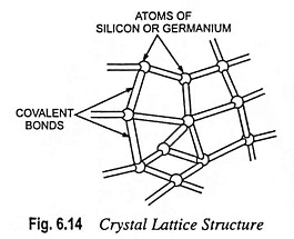
There are many semiconductor materials such as germanium, silicon, grey crystalline tin, selenium, tellurium, boron etc. available but silicon (Si) and germanium (Ge) are the two most widely used semiconductor materials in electronics. The reason for this is that energy required to break their covalent bonds (i.e., the energy required to release an electron from their valence bands) is very small (1.12 eV for silicon and 0.72 eV for germanium). Both elements have the same crystal structure (Fig. 6.14) and similar characteristics.
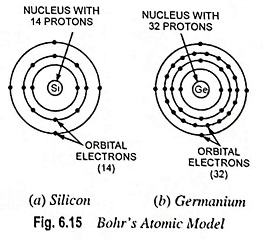
The atoms of silicon and germanium are illustrated in Fig. 6.15. It is seen that each of these atoms has four electrons in a valence shell that can have a maximum of eight. Thus, we say that their valence shells have four electrons and four holes. A hole is defined simply as an absence of an electron in a shell where one could exist.
Silicon is a tetravalent element and its atomic number is 14. It has, therefore, 14 protons and 14 electrons (two in first orbit, eight in second orbit and four in the third orbit), as shown in Fig. 6.15 (a).
Crystal lattice structure of silicon (also applicable to germanium) is shown in Fig. 6.14. Each atom is equidistant from its four neighboring atoms. In a crystalline structure each atom shares its four valence electrons with the four adjacent atoms. This occurs because each tetravalent semiconductor atom needs a total of eight outer-shell electrons. This sharing of electron pairs is called covalent bonding, already explained. The covalent bonds are illustrated in Fig. 6.14 by means of rods connecting the adjacent atoms. For simplified discussion, the crystal structure may be reduced to two dimensional. The core represents the nucleus and all the orbiting electrons except the valence electrons. Since there arc as many protons in the nucleus as there are electrons orbiting around it and there are four valence electrons, the core will have an excess +4 charge. The core of silicon contains 14 protons and 10 electrons (whereas germanium core has 32 protons and 28 electrons).
The energy band diagram for silicon is shown in Fig. 6.16 (a).
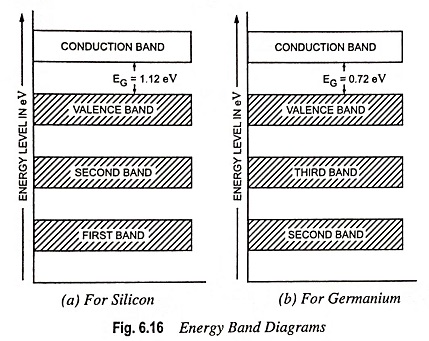
Germanium is also a tetravalent element i.e., it has 4 valence electrons. Its atomic number is 32. It has, therefore, 32, protons and 32 electrons [two in first orbit, eight in second orbit, eighteen in third orbit and four in fourth orbit], as shown in Fig. 6.15 (b). Its crystal lattice structure has already been discussed above. Energy band diagram for germanium is shown in Fig. 6.16 (b).
For semiconductors at a temperature of absolute zero (- 273.15°C) the valence band is usually full, and there may be no electrons in the conduction band. At absolute zero temperature EG for silicon and germanium are 1.21 eV and 0.785 eV respectively and it is difficult to get additional energy of this magnitude from applied electric field. Hence the conductivity of intrinsic semiconductors at absolute zero temperature is zero. However, at room temperature (300 K), the energy provided by the heat is sufficient to lift electrons from the valence band to the conduction band. Some electrons do jump the gap and go into the conduction band. So at room temperature, semiconductors are capable of conducting some electric current.
Since energy required in transferring electrons from valence band to conduction band is more in case of silicon than that in case of germanium, the conductivity of silicon will be less than that of germanium at room temperature.
Production of Holes and Free Electrons:
Breaking of covalent bond is equivalent to raising an electron from valence band to the conduction band. So the energy required to break a covalent bond is the same as the forbidden energy EG and equals 0.72 eV in case of germanium and 1.12 eV in case of silicon. This energy may be supplied either (i) by raising the temperature and thereby imparting thermal energy (ii) by incidence of photons in the visible range or (iii) by bombardment of the semiconductor materials by the α-particles, electrons and other particles and X-rays.
When an electron breaks a covalent bond of an intrinsic semiconductor and moves away, a vacancy is created in the broken covalent bond. The vacancy so caused constitutes a hole and is represented by a small circle. Whenever a free electron is generated, a hole is simultaneously created. Thus, free electrons and holes are always generated in pairs. So concentration of free electrons and holes will always he equal in an intrinsic semiconductor. Such generation of free electron-hole pairs is referred to as thermal generation. The formation of electron-hole pairs using crystal structure and energy band diagram is illustrated in Figs. 6.17 (a) and (b) respectively.
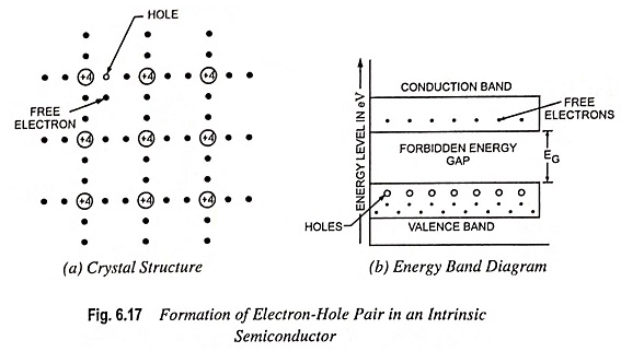
Since a crystal is electrically neutral, whenever an electron moves, a hole is left behind with a net positive charge equal in magnitude to that of negative charge of free electron.
Although, strictly speaking, a hole is not a particle; for all practical purposes it is viewed as a positively charged particle capable of conducting current. This concept of a hole as a positively charged particle merely helps in simplifying the explanation of conduction in semiconductors.
Carrier Generation and Recombination:
In an intrinsic semiconductor crystal equal number of free electrons and holes are created by thermal (heat) energy. The reason being that a hole is created only by removing an electron from the covalent bond. Thus the electrons and holes arc created in pairs. Since the free electrons and holes move randomly within the crystal lattice, there is always a possibility of an electron meeting a hole. Although this possibility is small, even then when a free electron approaches the hole, it gets attracted and falls into the hole. This merging of a free electron and a hole is called recombination. In this process of recombination, both the free electron and hole disappear and energy is released as a quantum heat or light. The energy so released may in turn be re-absorbed by another electron to break away from its valence band and create a new electron-hole pair.
The recombination rate is proportional to the product of the concentrations or densities of free electrons and holes. Thus the processes of breaking of covalent bonds and recombination of electrons and holes take place simultaneously. The amount of time between the creation and disappearance of a free electron is called the lifetime. It varies from a few nanoseconds to several microseconds, depending how perfect the crystal is and other factors.
The rate of production of electron-hole pairs increases with the rise in temperature; the rate of recombination is proportional to the product of concentrations of free electrons and holes and at a given temperature, the concentrations or densities of free electrons and holes remain fixed and equal. So the rate of generation of electron-hole pairs must be equal to the rate of their recombination. With the increase in temperature, the rate of generation of electron-hole pairs increases. The concentration of electrons and holes goes on increasing until rate of recombination equals the increased rate of generation. Thus with the increase in temperature, concentrations of free electrons and holes increase.
Conduction in Intrinsic Semiconductors:
When the electrons are liberated on breaking of covalent bonds, they move randomly through the crystal lattice. These free electrons are neither attracted by the nuclei of the atoms nor repelled by the electrons bound by covalent bonds because their electrical effects are fully engaged in maintaining the covalent bonds. When an external electric field is applied to a pure (intrinsic) semiconductor, the conduction through the semiconductor is by both free electrons and holes. The free electrons in the conduction band move towards the positive terminal of the battery while the holes in the valence band move towards the negative terminal of the battery i.e., the electrons and holes move in opposite directions. As the holes reach the negative terminal B, the electrons reaching there combine with the holes which are thus destroyed. At the same time, the loosely held electrons near the positive terminal A are attracted away from their atoms into the positive terminal of the battery. Now new holes are created which again drift towards the negative terminal B. The electric current flows through the intrinsic semiconductor in the same direction as in which the holes are moving (the holes having positive charge). Since electrons are negatively charged, the direction of conventional current is opposite to that of movement of electrons. The total current inside the conductor is thus the sum of currents owing to free electrons and holes (though the two types of charge carriers move in the opposite directions) but current in the external wires is only because of electrons, as illustrated in Fig. 6.18.
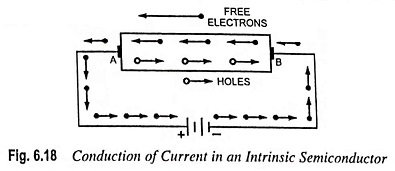
The mobility of electrons is more than that of holes because the probability of an electron having the energy required to move to an empty state in the conduction band is much greater than the probability of an electron having the energy required to move to the empty state in valence band. Thus the current due to movement of electrons is greater than that due to the hole drift in the semiconductor. The mobility of hole is about half that of an electron. The net current is very small.
Effects of Heat and Light on Conductivity of Intrinsic Semiconductors:
At absolute zero temperature (-273°C), all the electrons of intrinsic semiconductors (germanium or silicon) are tightly held by their atoms. The inner orbit electrons are bound to nucleus whereas the valence electrons are bound by the forces of covalent bonds. Thus, at absolute zero temperature, no free electron is available in the intrinsic semiconductor and so it behaves like a perfect insulator.
When the material is heated, electrons break away from their atoms and move from the valence band to conduction band. This produces holes in the valence band and free electrons in the conduction band. Conduction can then occur by electron movement and by hole transfer. With the increase in temperature, the rate of generation of electron-hole pairs is increased. This in turn increases the rate of recombination. Thus with the increase in temperature, the concentration of charge carriers (electrons and holes) increases. As more charge carriers are made available, the conductivity of a pure semiconductor increases with the increase in temperature. In other words resistivity of a pure semiconductor decreases with the increase in temperature i.e., the semiconductors have negative temperature coefficient of resistance.
When the semiconductor is illuminated, its resistance decreases in the same way as in case of increase in temperature.
The forbidden energy gap EG also depends somewhat on temperature. It has been determined experimentally that EG for semiconductors decreases with the increase in temperature. For example EG for Si becomes 1.12 eV and that for Ge becomes 0.72 eV at room temperature while the respective values at absolute zero temperature are 1.21 eV and 0.785 eV.
The resistance of a semiconductor depends largely on
- temperature—decreases with the increase in temperature,
- illumination—decreases in brighter surroundings and
- magnitude of the electric field—the current does not increase in proportion to the applied potential, as in case of conductors obeying Ohm’s law, but increases by far more than the voltage i.e., the semiconductors are nonlinear.
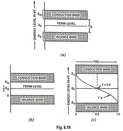
Fermi Level in an Intrinsic Semiconductor:
The Fermi level is simply a reference energy level. It is the energy level at which the probability of finding an electron n energy units above it in the conduction band is equal to the probability of finding a hole (electron absence) n energy units below it in the valence band. Very simply, it can be considered to be the average energy level of the electrons, as illustrated in Fig. 6.19 (a).
Let at any temperature T K
- Number of electrons in the conduction band be nC
- Number of electrons in the valence band be nV
- Total number of electrons in both bands, n = nC + nV
For simplification let us assume that (i) widths of energy bands are small in comparison to forbidden energy gap between them (ii) all levels in a band have the same energy, bandwidths being assumed to be small (iii) energies of all levels in valence band are E0, as shown in Fig. 6.19 (a) and (iv) energies of all levels in conduction band are EG.
Let the zero-energy reference level be taken arbitrarily at the top of the valence band, as shown in Fig. 6.19 (b).
Now number of electrons in conduction band,
![]()
where P(EG) represents the probability of an electron having energy EG. Its value may be determined from Fermi-Dirac probability distribution function given as
where P(E) is the probability of finding an electron having any particular value of energy E.
![]()
where EF is the Fermi level.
Substituting the value of P(EG) from Eq. (6.13) in Eq. (6.11), we have
![]()
Now number of electrons in valence band,
![]()
The probability P(0) of an electron being found in the valence band with zero energy can be determined by substituting E = 0 in Eq. (6.12)
Now total number of electrons in both bands,
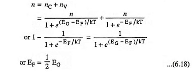
i.e., in an intrinsic semiconductor, the Fermi level lies midway between the conduction and valence bands.