Conductor Semiconductor and Insulator:
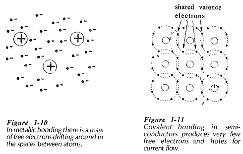
Bonding Forces Between Atoms: Whether a material is a Conductor Semiconductor and Insulator depends largely upon what happens to the outer-shell electrons when the atoms bond themselves together to form a solid. In the case of copper, the easily detached valence electrons are given up by the atoms. As illustrated in Fig. 1-10, this creates a great mass of free electrons (or electron gas) drifting about in the space between the copper atoms. The electrons are easily moved under the influence of an applied voltage to create a current flow. The bonding force that holds atoms together in a conductor is known as metallic bonding.
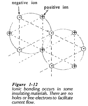
Semiconductor atoms normally have four outer-shell electrons and four holes, and are so close together that the outer-shell electrons behave as if they were orbiting in the valence shells of two atoms. In this way each valence-shell electron fills one of the holes in the valence shell of a neighboring atom. This produces an atomic bonding force known as covalent bonding. As shown in Fig. 1-11, it would appear that there are no holes and no free electrons drifting about within the semiconductor material. In fact, some of the electrons are so weakly attached to their atoms that they can be made to break away to create a current flow when a voltage is applied.
In some insulating materials the atoms bond together in a similar way to semiconductor atoms (covalent bonding). But the valence shell electrons are so strongly attached to their atoms in an Insulator that no charge carriers are available for current flow. In other types of insulating materials, some atoms give up outer shell electrons which are accepted into the orbit of neighboring atoms. Because the atoms are ionized, this is termed ionic bonding, (Fig. 1-12). Here in Conductor Semiconductor and Insulator again, all of the electrons are very strongly attached to the atoms, and the possibility of current flow is virtually zero.
Energy Band Diagram for Conductors Insulators and Semiconductors:
The Energy Band Diagram for Conductors Insulators and Semiconductors is shown in Fig. 1-13 show that insulators have a wide forbidden gap, semiconductors have a narrow forbidden gap, and conductors have no forbidden gap at all.
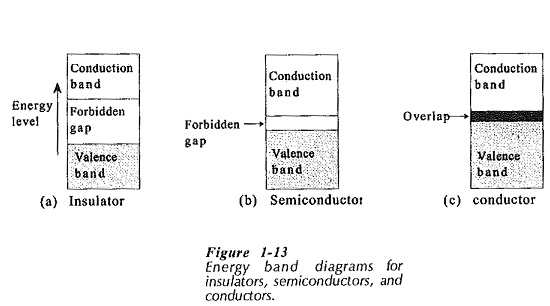
In the case of insulators, there are practically no electrons in the conduction band, and the valence band is filled. Also, the forbidden gap is so wide [Fig. 1-13(a)] that it would require the application of relatively large amounts of energy to cause an electron to cross from the valence band to the conduction band. Therefore, when a voltage is applied to an insulator, conduction cannot normally occur either by electron motion or hole transfer.
For semiconductors at absolute zero of temperature (-273°C) the valence band is usually full and there may be no electrons in the conduction band. As shown in Fig. 1- 13(b), the forbidden gap in a semiconductor is very much narrower than that in an insulator, and the application of small amounts of energy can raise electrons from the valence band to the conduction band. Sufficient thermal energy for this purpose is available when the semiconductor is at normal room temperature. If a voltage is applied to the semiconductor, conduction can occur by both electron movement in the conduction band and by hole transfer in the valence band.
In the case of a conductor [Fig. 1-13(c)] there is no forbidden gap, and the valence and conduction energy bands overlap. For this reason, very large numbers of electrons are available for conduction, even at extremely low temperatures.
Typical resistance values for a 1-centimeter-cube sample are: Conductor 10-6Ω, Semiconductor 10 Ω, Insulator 1014 Ω.