P Type and N Type Semiconductor:
Doping : Pure semiconductor material is known as intrinsic material. Before intrinsic material can be used for device manufacture, impurity atoms must be added to improve its conductivity. The process of adding the atoms is termed doping. Two different types of doping are possible; donor doping, and acceptor doping. Donor doping generates free electrons in the conduction band (i.e., electrons that are not tied to an atom). Acceptor doping produces valence band holes, or a shortage of valence electrons in the material. After doping, the semiconductor is known as extrinsic material. Two types of extrinsic semiconductor are P Type and N Type Semiconductor.
N Type semiconductor Diagram:
In donor doping, illustrated in Fig. 1-14, impurity atoms which have five electrons and three holes in their valence shells are added to the undoped material. The impurity atoms form covalent bonds with the silicon or germanium atoms. Because the semiconductor atoms have only four electrons and four holes in their valence shells, there is one extra valence-shell electron for each impurity atom added. Each additional electron produced in this way enters the conduction band as a free electron. As shown in Fig. 1-14, there is no hole for the fifth electron from the outer shell of the impurity atom; therefore, this electron becomes a free electron. Because the free electrons have negative charges, donor-doped semiconductor is known as n-type material.
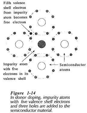
Free electrons in the conduction band are easily moved around under the influence of an electric field. Consequently, conduction occurs largely by electron motion in donor-doped semiconductor material. The doped material remains electrically neutral (it is neither positively charged nor negatively charged), because the total number of electrons (including the free electrons) is still equal to the total number of protons in the atomic nuclei.
The term donor doping comes from the fact that an electron is donated to the conduction band by each impurity atom. Typical donor materials are antimony, phosphorus, and arsenic. Since these atoms have five valence electrons, they are referred to as pentavalent atoms.
P Type Semiconductor Diagram:
The impurity atoms used for acceptor doping (Fig. 1-15) have outer shells containing three electrons and five holes. Suitable atoms with three valence electrons (trivalent atoms) are boron, aluminum, and gallium. These atoms form covalent bonds with the semiconductor atoms, but the bonds lack one electron for complete outer shell of eight. In Fig. 1-15 the impurity atom illustrated has only three valence electrons; so, a hole exists in its bond with the surrounding atoms. thus, in acceptor doping, holes are introduced into the valence band, so that conduction may occur by the process of hole transfer.
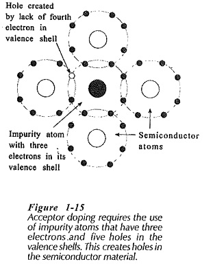
Since holes can be said to have a positive charge, acceptor-doped semi-conductor material is referred to as p-type material. As with n-type, the material remains electrically neutral, because the total number of orbital electrons in each impurity atom is equal to the total number of protons in its atomic nucleus. Holes can accept a free electron, hence the term acceptor doping.
Majority and Minority Carriers in PN Junction:
In undoped semiconductor material at room temperature there are a number of free electrons and holes. These are due to thermal energy causing some electrons to break the bonds with their atoms and enter the conduction band. This process creates pairs of holes and electrons, and is appropriately termed hole-electron pair generation. The opposite effect, called recombination, occurs when an electron falls into a hole in the valence band. Because there are many more electrons than holes in n-type material, electrons are said to be the majority charge carriers, and holes are said to be minority carriers in n-type material. In p-type material, holes are the majority carriers and electrons are minority carriers.
Heat and light effect on semiconductors:
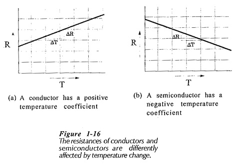
When a conductor is heated, the atoms (which are in fixed locations) tend to vibrate, and the vibration impedes the movement of the surrounding electron gas. This causes a reduction in the flow of the electrons that constitute the electric current. The reduced current flow means that the conductor resistance has increased. A conductor has a Positive Temperature Coefficient (PTC) of resistance; a resistance which increases with increasing temperature. This is illustrated in Fig. 1-16(a).
When undoped semiconductor material is at a temperature of absolute zero (-273°C), all electrons are in normal orbit around the atoms, and there are virtually no free electrons in the conduction band and no holes in the valence band. Consequently, at -273°C a semiconductor behaves as an insulator.
When the P Type and N Type Semiconductor temperature is raised, electrons break away from their atoms and move from the valence band to the conduction band. This produces holes in the valence band and free electrons in the conduction band, allowing conduction to occur by electron movement and by hole transfer. Increasing application of thermal energy generates an increasing number of hole-electron pairs.
As in the case of a conductor, thermal vibration of atoms occurs in a semiconductor. However, there are very few electrons to be impeded in a semiconductor compared to the large quantities in a conductor. The thermal generation of electrons is the dominating factor, and the semiconductor current increases with increasing temperature. This represents a decrease in resistance with increasing temperature; a Negative Temperature Coefficient (NTC), Fig [1-16(b)]. Heavily doped semiconductor material is an exception, behaving more like a conductor than a semiconductor.
Just as thermal energy can cause electrons to break their atomic bonds, so hole-electron-pairs can be generated by energy applied to a P Type and N Type Semiconductor in the form of light. A material which has few free electrons available for conduction when not illuminated is said to have a High Dark Resistance. When the P Type and N Type Semiconductor material is illuminated, its resistance decreases and may become comparable to that of a conductor.