PN Junction Forward Bias:
Consider the effect of an external bias voltage applied with the polarity of PN Junction Forward Bias shown in Fig. 1-23; positive on the p-side, negative on the n-side. The holes on the p-side, being positively charged particles, are repelled from the positive terminal and driven toward the junction.
Similarly, the electrons on the n-side are repelled from the negative terminal toward the junction. The result is that the depletion region width and the bather potential are both reduced.
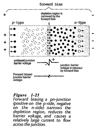
When the applied bias voltage is progressively increased from zero, the barrier voltage gets smaller until it effectively disappears and charge carriers easily flow across the PN Junction Forward Bias. Electrons from the n-side are now attracted across to the positive bias terminal on the p-side, and holes from the p-side flow across to the negative terminal on the n-side, (thinking of holes as positively-charged particles). Thus, a majority carrier current flows, and the junction is said to be PN Junction Forward Bias.
Forward Bias Characteristics:
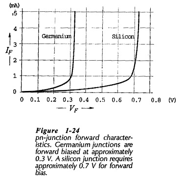
The graph in Fig. 1-24 shows the forward current (IF) plotted against forward voltage (VF) for typical germanium and silicon pn-Junctions. In each case, the graph is known as the forward characteristic of the junction. It is seen that very little forward current flows until VF exceeds the junction barrier, voltage (0.3 V for germanium, 0.7 V for silicon).
When VF is increased from zero toward the knee of the characteristic, the barrier voltage is progressively overcome, allowing more majority charge carriers to flow across the junction. Above the knee of the characteristic IF increases almost linearly with increase in VF. The level of current that can be made to flow across a forward-biased pn-junction largely depends on the junction area.