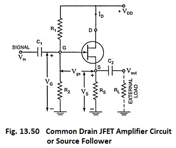
Common Drain JFET Amplifier or Source Follower:
In the Common Drain JFET Amplifier circuit (also called the source follower), the output voltage is developed across source resistor RS. External load resistor RL is connected to FET source terminal S through coupling capacitor C2, and gate bias voltage VG is derived from VDD by means of potential divider R1 and R2. No resistor is connected in series with the drain terminal, and no source bypass capacitor is used. The input signal is applied to the gate through coupling capacitor C1.
For understanding the operation of the common drain circuit, note that gate voltage VG is a constant quantity, as in any potential divider bias circuit. When a signal is applied to the FET gate through C1, gate voltage increases and decreases as the input signal goes positive and negative respectively.
Also Vgs remains substantially constant, therefore, the source voltage Vs increases or decreases with the increase or decrease in gate voltage. Since the FET source is the output terminal, it is seen that the output voltage from a common drain circuit is approximately the same as the input voltage. Thus, the common drain circuit can be said to have approximately unity gain. Because the output voltage at the FET source terminal follows variations in the signal voltage applied to the gate, the common drain circuit is also known as a source follower.
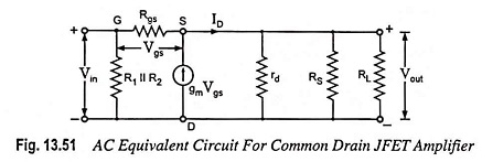
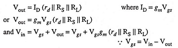
The Common Drain JFET Amplifier ac equivalent circuit is shown in Fig. 13.51. The current generator is gmVgs where Vgs = Vin – Vout. Moreover RG = R1 || R2.
Voltage gain
![]()
Normally rd ≫ RS || RL
![]()
If gm (RS || RL) ≫ 1 then Av ≈ 1
So value of voltage gain becomes approximately equal to unity (slightly less than unity).
Input Impedance: The circuit input impedance is RG = R1 || R2.
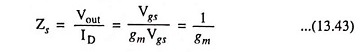
Output Impedance: In a Source Follower circuit, any variation in output voltage Vout affects upon the gate-source voltage Vgs and Vgs is given as
![]()
Normally Rgs ≫ Rs || RG, so Vgs = Vout
and
![]()
Also
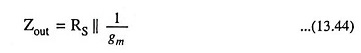
Actually, rd is in parallel with 1/gm, but since rd ≫ 1/gm, it is neglected. Rs is the output impedance of the device. The circuit output impedane