Common Source Circuit Analysis:
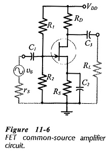
A FET Common Source Circuit Analysis is shown in Fig. 11-6. With the capacitors treated as ac short-circuits, the circuit input terminals are the gate and source, and the output terminals are the drain and the source. So, the source terminal is common to both input and output, and the circuit configuration is known as common-source (CS).
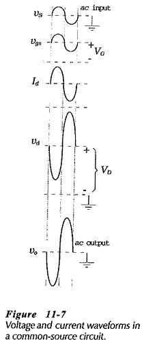
The current and voltage waveforms for the CS circuit in Fig. 11-6 are illustrated in Fig. 11-7. The 180° phase shift between the input and output waveforms can be understood by considering the effect of a positive-going input signal. An increase in vs increases the FET gate-source voltage (VGS), thus raising the level of ID, and increasing the voltage drop across RD. This produces a decrease in the level of the drain voltage (VD), which is capacitor-coupled to the circuit output as a negative-going ac output voltage (vo). Consequently, as vs increases in a positive direction, vo changes in a negative direction, as illustrated. Conversely, when vs changes in a negative direction, the resultant decrease in VGS reduces ID, and produces a positive-going output.
The circuit in Fig. 11-6 has an input impedance (Zi), an output impedance (Zo), and a voltage gain (Av). Equations for these quantities can be determined by ac analysis of the circuit.
Common Source Equivalent Circuit:
The first step in ac analysis of a FET (or BJT) circuit is to draw the ac equivalent circuit, by substituting ac short-circuits in place of the power supply and capacitors. When this is done for the circuit in Fig. 11-6, the at equivalent circuit shown in Fig. 11-8(a) is created. For ac analysis, the FET equivalent circuit [from Fig. 115(b)] is now substituted in place of the device. This results in the CS at equivalent circuit in Fig. 11-8(b).
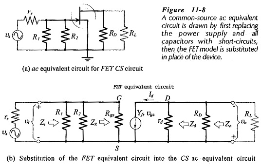
The current directions and voltage polarities in Fig. 11-8(b) are those that occur when the instantaneous level of the input voltage is moving in a positive direction.
Input Impedance:
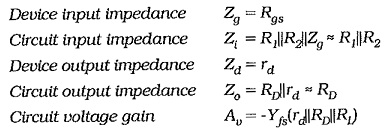
Considering the input section of the equivalent circuit in Fig. 11-8(b) it is seen that the input impedance at the FET terminals is,
![]()
As already discussed, a typical value of Rgs for a low-current JFET is 109 Ω. At the circuit input terminals, resistors R1 and R2 are seen to be in parallel with Zg. So, the circuit input impedance is
![]()
Because Zg is so large, the circuit input impedance is almost always determined by the bias resistors.
![]()
So, the input impedance of a FET circuit can usually be determined simply by calculating the equivalent resistance of the bias resistors. However, as already discussed, very high input resistance is one of the most important properties of a FET. In circumstances where it is necessary to achieve the highest possible input resistance, the signal source might be directly connected in series with the gate terminal, and in this case Zi ≈ Zg.
Output Impedance:
Looking into the output of the CS equivalent circuit in Fig. 11-8(b), the output impedance at the FET drain terminal is,
![]()
At the circuit output terminals, resistor RD is in parallel with Zd. So, the circuit output impedance is,
![]()
Because rd is typically 100 kΩ and RD is usually much lower than 50 kΩ, the circuit output impedance is approximately equal to RD. Using this information, the output impedance of a CS circuit can be discovered simply by reading the resistance of RD.
![]()
Voltage Gain:
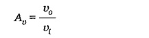
Amplifier voltage gain is given by the equation,
From Fig. 11-8(b),
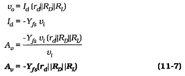
The minus sign in Eq. 11-7 indicates that vo is 180° out of phase with vi. (When vi increases, vo decreases, and vice versa.) It is seen that the voltage gain of a Common Source Circuit Analysis is directly proportional to the Yfs of the FET. If the appropriate Yfs value and the resistance of RD and RL are known, the voltage gain of a CS circuit can be quickly estimated. For Yfs = 5000 μS, RD = 4.7 kΩ, and with RL ≫ RD, and rd ≫ RD, the voltage gain is -23.5.
The voltage gain of a FET Common Source Circuit Analysis is typically about one tenth of the gain of a BJT common-emitter circuit. Low voltage gain, caused by the low Yfs value, is the major disadvantage of JFET circuits compared to BJT circuits. The same is generally true of MOSFET circuits, except for E-MOSFET devices (V-MOS and T-MOS), which have much larger Yfs values. However, E-MOSFETs use relatively large drain currents, and they are normally unsuitable for small-signal applications.
Summary of Typical CS Circuit Performance:
The Common Source Circuit Analysis has voltage gain,180° phase shift, high input impedance, and relatively high output impedance.