Common Gate JFET Amplifier and its AC Equivalent Circuit:
The circuit of a simple Common Gate JFET Amplifier is shown in Fig. 13.53 and its ac equivalent circuit is shown in Fig. 13.54. In this Amplifier Circuit, input signal is applied to the source terminal S and output is taken from the drain terminal D, as illustrated in Fig. 13.53.
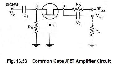
The gate is grounded and external load resistor RL is connected to the drain terminal D through coupling capacitor C2. In ac equivalent circuit, current source is connected between the drain and source terminals, as usual. However, since source and drain are the input and output terminals respectively, gmVgs appears between the input and output.
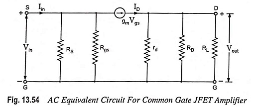
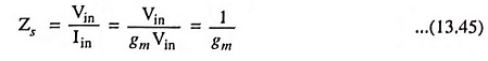
Input Impedance: Ignoring current through RS and Rgs, the input current
![]()
So input impedance of FET,
The input impedance of the circuit is Zs || RS. So,
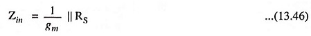
Actually speaking rd and RD are also involved in Zin but their effect is negligible.
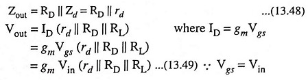
Output Impedance: The output of a Common Gate JFET Amplifier Circuit is taken from the drain terminal, just as in the case of a common source circuit. So the output impedance at the drain terminal is
![]()
Again this equation gives the impedance looking into the device drain terminal. The circuit output impedance
Voltage gain,
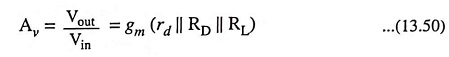
Usually rd ≫ RD || RL
So
![]()
The above equation for voltage gain is the same as that in case of a common source circuit, except that there is no minus sign. It means that output voltage and input voltage are in phase.