Coupling Capacitors:
Coupling Capacitors are required at a circuit input to couple a signal source to the circuit without affecting the bias conditions. Similarly, loads are capacitor-coupled to the circuit output to avoid the change in bias conditions produced by direct coupling. Input and output Coupling Capacitors (C1 and C3) and are shown in the FET circuit in Fig. 11-1.
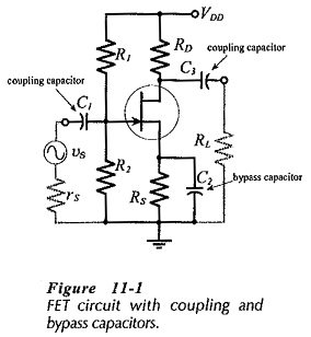
Bypassing Capacitors:
Bypass capacitors are also just as necessary in FET circuits as in BJT circuits. Bypass capacitor C2 in Fig. 11-1 provides an ac short-circuit across resistor RS. As will be shown, if C2 is not present RS substantially reduces the ac voltage gain of the circuit.
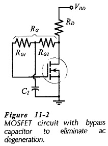
Figure 11-2 illustrates another situation where a bypassing capacitor is required. The MOSFET drain-to-gate bias circuit shown would have its voltage gain reduced by feedback from the drain to the gate via RG (ac degeneration) if capacitor C2 were not present. Splitting RG into two equal resistors and ac shorting the junction to ground via C2 eliminates the feedback.
AC Load Lines:
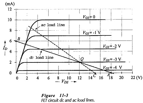
Once again, this is a subject that applies equally to BJT and FET circuits. The dc load for the FET circuit in Fig. 11-1 is (RD + RS). With RS ac bypassed and R L absent, the ac load is RD. With the Coupling Capacitors load present in Fig. 11-1, the ac load is RD||RL. The dc load line is drawn in the usual way, and the Q-point is marked, then the ac load line is drawn through the Q-point, as shown in Fig. 11-3.