Darlington Amplifier – Circuit Diagram, Characteristics, Merits and Applications:
Darlington amplifier with voltage divider bias is shown in Fig. 19.50. In this circuit the output of one amplifier is coupled into the input of the next one by directly joining emitter of one transistor to the base of the other one, as shown in the figure. Obviously, the emitter current of the first transistor becomes the base current for the second transistor.
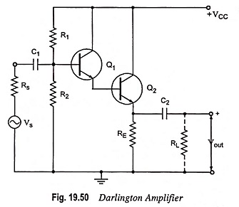
The biasing analysis is similar to that for one transistor except that two VBE drops are to be considered.
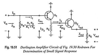
The Darlington amplifier circuit in its small signal ac form will appear, as shown in Fig. 19.51.
Main Characteristics:
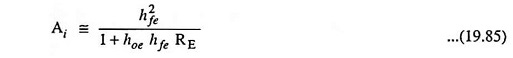
1. Current Gain: For the second stage:
Input impedance,
![]()
and current gain,

On a good approximate basis, these equations cannot be applied to the first stage. The “fly in the ointment” is the closeness with which Zin2 compares with 1/hoe1. We have seen that 1/hoe, could be eliminated in the majority of the cases because the load impedance ZL << 1/hoe. For the Darlington Amplifier circuit the input impedance Zin2 is close enough in magnitude to 1/hoe to necessitate considering the effects of hoe1. We already discussed that, it was found that for single stage grounded emitter transistor amplifier, where 1/hoe was considered,

Applying the above equation to this situation,
and current gain,
![]()
Current gain,
For hoehfeRE ≤ 0.1, a fairly good approximation (within 10%) is
![]()
Alternatively current gain can be obtained as follows:
Emitter current,
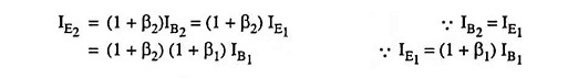
So current gain,

It means Darlington amplifier behaves like a single transistor having current gain equal to β2.
2. Input Impedance: Since Zin2 = hfe2RE is the emitter resistance of the first stage, the input impedance to the first stage is

Since Zin2 = hfe2RE, and 1/hoe1 will appear in parallel in the small signal equivalent circuit, so
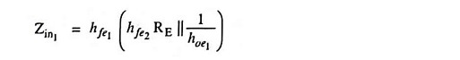
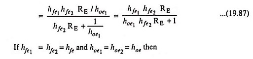
Input impedance,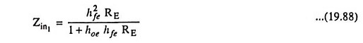
![]()
Alternatively input impedance can be obtained as follows:
Input impedance of second stage,
![]()
where r′e2 is the ac emitter resistance of second transistor.
If RE >> r′e2, then Zin2 = β2RE
Zin2 is also the output impedance while looking into the emitter of first transistor. So input impedance looking into the base of first transistor,
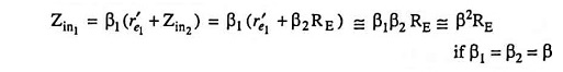
This input impedance is very high because of the product of two betas,
so input impedance,
![]()
If there is a load resistance RL coupled to the emitter of second transistor, then
![]()
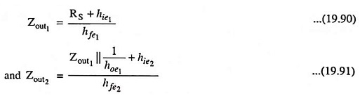
3. Output Impedance: The output impedance Zout can be determined directly from the emitter equivalent circuits as follows:
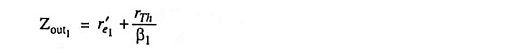
Alternatively the output impedance Zout can be determined as follows :
The ac Thevenin’s impedance at the input rTh = Rs||R1||R2 because by shorting all voltage sources R1 and Rs comes in parallel with R2
Output impedance of first stage,
Output impedance of second stage,

Zout2 is quiet smaller than Zout1 i.e., output impedance is lowered.
Because of this, Darlington amplifier can be used to isolate high impedance source from low impedance load. If high impedance source is directly connected to a low impedance load, most of the signal voltage will be dropped across the high impedance of the source and remaining source signal available may not be able to drive the load.
4. Voltage Gain: Applying Kirchhoff’s voltage law to the circuit shown in Fig. 19.50.
![]()
That the output potential is the input potential less the base-to-emitter potential of each transistor. It clearly indicates that Vout < Vin. Voltage gain is closer in magnitude to one than to zero.
On an approximate basis it is given as
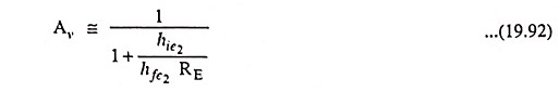
On an approximate basis voltage gain can be determined from the following relation also
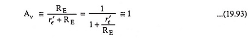
(slightly less than unity) as in case of emitter follower
Note : r′e1 and r′e2 have been assumed to be equal and each one equal to r′e.
Merits:
- It uses very few components and can be readily formed from two adjacent transistors in an IC.
- It provides excellent characteristics of high input impedance with low output impedance and high current gain, all desirable characteristics for a current gain amplifier.
Applications of Darlington Amplifier:
It has enormous impedance transformation capability i.e., it can transform a low impedance load to a high impedance load. Hence it is used in a high gain operational amplifier which depends on very high input impedance for its operation as an integrator or summing amplifier in analogue applications.