Diode Clipping Circuit – Types and Applications:
Diode Clipping Circuit – For a clipping circuit at least two components—an ideal diode and resistor are required and sometimes a dc battery is also employed for fixing the clipping level. The diode acts as a closed switch when forward biased and an open switch when reverse biased. The input waveform can he clipped at different levels by simply changing the voltage of the battery and by interchanging the positions of the various elements.
Depending on the orientation of the diode, the positive or negative region of the input signal is “clipped” off and accordingly the diode clippers may be positive or negative clippers.
There are two general categories of clippers: series and parallel (or shunt). The series configuration is defined as one where diode is in series with the load, while the shunt clipper has the diode in a branch parallel to the load.
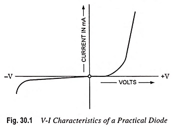
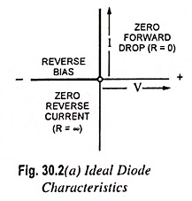
V-I characteristics of a practical diode are depicted in Fig. 30.1. V-I characteristics of an idealized diode (approximated by a curve which is piecewise linear and continuous) are shown in Figs. 7.10 (b), 7.11 and 7.22 and repeated for easy reference in Figs. 30.2 (a), (b) and (c) respectively. The idealized diode characteristic exhibits a discontinuity in slope at the voltage Vγ, and this point of slope discontinuity is called a break point. The break point occurs at Vγ = 0.2 V for germanium and Vγ = 0.6 V for silicon. For a backward diode, Vγ is almost zero.
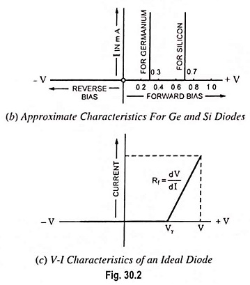
Using the piecewise linear model of a diode, the Diode Clipping Circuit given in Fig. 30.3 (b) has the transmission characteristic depicted in Fig. 30.3 (c). The transmission characteristic – a plot of the output voltage Vout against the input voltage vin also exhibits piecewise linear discontinuity. A break point occurs at the voltage V + Vγ. To the left of the break point [for vin < (V + Vγ)], the diode is reverse biased (off). In this region, the input signal vin may be transmitted directly to the output, as there is no load across the output to cause a drop across the series resistor R. To the right of the break point [for vin > (V + Vγ)], the diode is forward biased (on) and increments Δvin in the input are attenuated and appear at the output as increment Δvout = Δvin x Rf/Rf+R, in which R is the diode forward resistance.
Figure 30.3 (c) depicts a sinusoidal input signal of amplitude large enough so that the signal makes excursions past the break point. The corresponding output exhibits a suppression of positive peak of the signal. In case forward resistance Rf is much smaller than series resistance R(Rf << R), this suppression will be very pronounced, and the positive output excursion will be sharply limited at the voltage V + Vγ. The output will appear as if the positive peak had been ‘clipped off’ or ‘sliced off’. Usually Vγ is negligibly small in comparison with reference voltage V. In such a case one may consider that V itself is the limiting reference voltage.
Positive Clipper:
The clipper which removes the positive half cycles of the input voltage is called the positive clipper. The circuit arrangements for a positive clippers are illustrated in Fig. 30.4.
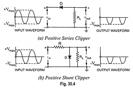
Figure 30.4 (a) illustrates the positive series clipper circuit (i.e., diode in series with the load). From the Fig. 30.4 (a) it is seen that while the input is positive, diode D is reverse biased and so the output remains at zero i.e., positive half cycle is “clipped“ off. During the negative half cycle of the input, the diode is forward biased and so the negative half cycle appears across the output.
Figure 30.4 (b) illustrates the positive shunt clipper circuit (i.e., diode in parallel with the load). From the Fig. 30.4 (b) it is seen that while input side is positive, the diode D is forward biased and conducts heavily (i.e., diode acts as a closed switch). So the voltage drop across the diode or across the load resistance RL is zero. Thus output voltage during the positive half cycles is zero, as shown in the output waveform. During the negative half cycles of the input signal voltage, the diode D is reverse biased and behaves as an open switch. Consequently the entire input voltage appears across the diode or across the load resistance RL if R is much smaller than RL.
Actually the circuit behaves as a voltage divider with an output voltage of -RL/R+RL Vmax ≈-Vmax when RL≫ R.
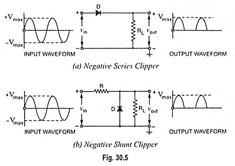
Note : If the diode in Figs. 30.4 (a) and 30.4 (b) is reconnected with reversed polarity, the circuits will become for a negative series clipper and negative shunt clipper respectively.
The negative series and negative shunt clippers are shown in Figs. 30.5 (a) and 30.5 (b) respectively. The negative clipper is one which removes all the negative half cycles of the input voltage.
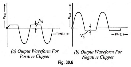
In the above discussion, the diode is considered to be ideal one. If second approximation for diode is considered the barrier potential, V0 (0.7 V for silicon and 0.3 V for Ge) of diode, will be taken into account. Then the output waveforms for positive and negative clippers will be of the shape shown in Fig, 30.6.
Biased Clipper:
Sometimes it is desired to remove a small portion of positive or negative half cycles of the signal voltage. Biased clippers are employed for this purpose.. The circuit diagram for a biased negative clipper (i.e., for removing a small portion of each negative half cycle) is illustrated in Fig. 30.7 (a). The action of the circuit is explained below.
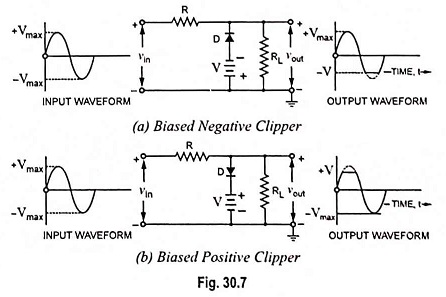
When the input signal voltage is positive, the diode D is reverse biased and behaves as an open switch, the entire positive half cycle appears across the load, as illustrated by output waveform [Fig. 30.7 (a)]. When the input signal voltage is negative but does not exceed battery voltage V, the diode D remains reverse biased and most of the input voltage appears across the output. When during the negative half cycle of input signal, the signal voltage exceeds the battery voltage V, the diode D is forward biased i.e., conducts heavily. The output voltage is equal to -V and stays at -V as long as the input signal voltage is greater than battery voltage V in magnitude. Thus a biased negative clipper removes input voltage when the input signal voltage exceeds the battery voltage. Diode Clipping Circuit can be changed by reversing the battery and diode connections, as illustrated in Fig. 30.7 (b).
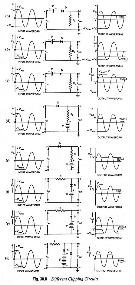
Sonic of other biased clipper circuits are given in Fig. 30.8. While drawing the waveshape of the output basic principles discussed above are followed. The diode has been considered as an ideal one.
Combination Clipper:
When a portion of both positive and negative of each half cycle of the input voltage is to be clipped (or removed), combination clipper is employed. Such Diode Clipping Circuit is given in Fig. 30.9. The action of the circuit is summarized below
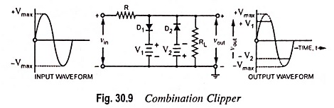
For positive input voltage signal when input voltage exceeds battery voltage +V1, diode D1 conducts heavily while diode D2 is reverse biased and so voltage +V1 appears across the output. This output voltage +V1 stays as long as the input signal voltage exceeds +V1. On the other hand for the negative input voltage signal, the diode D1 remains reverse biased and diode D2 conducts heavily only when input voltage exceeds battery voltage V2 in magnitude.
Thus during the negative half cycle the output stays at -V2 so long as the input signal voltage is greater than -V2.
Zener Diode as a Peak Clipper:
Zener diodes can be used for clipping off the input waveform in waveshaping circuits, as illustrated in Fig. 30.10.
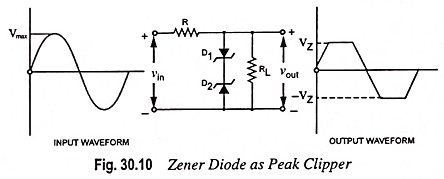
Two similar zener diodes D1 and D2 are shunted across the input sinusoidal voltage of peak value of Vmax volts. Let the zener voltage of each of zener diodes be VZ volts (VZ being lesser than Vmax).
We have seen that a zener diode acts like a ‘short’ (or very low resistance) when forward biased and ‘open’ (or very high resistance) when reverse biased till it goes into breakdown at VZ. The action of the circuit is explained below.
For positive input half cycle diode D1 is forward biased and acts like a ‘short’ while diode D2 acts like an open (being reverse biased) up to VZ. Thereafter diode D2 goes into breakdown and holds the output voltage constant at VZ till input voltage falls below VZ in the later part of the positive half cycle. This is because during this duration of time both of the diodes act as ‘short’. When the supply voltage falls below VZ, diode D2 comes out of the breakdown and again acts as an open across the load circuit. During the negative input half cycle, the actions of diodes D1 and D2 are reversed. The result is that the output voltage waveform is clipped off on both peaks, as illustrated in Fig. 30.10.
Drawbacks of Series and Shunt Diode Clipping Circuit:
In series clippers, when diode is in ‘off’ position, there should be no transmission of input signal to output. But in case of high-frequency signals transmission occurs through diode capacitance which is undesirable. This is the drawback of using diode as a series element in such clippers.
In shunt clippers, when diode is in the ‘off’ condition, transmission of input signal should take place to output. But in case of high-frequency input signals, diode capacitance affects the circuit operation adversely and the signal gets attenuated (i.e., it passes through diode capacitance to ground).
Applications of Diode Clipping Circuit:
There are numerous applications and it is beyond the scope of the book to discuss or enumerate all of them. They find wide application in television receivers for separating synchronizing signals from composite picture signals and also in television transmitters at the time of processing the picture signals. They are also employed for generation of different waveforms, such as trapezoidal, square or rectangular waves. Series clippers are employed as noise limiters in FM transmitters by clipping excessive noise peaks above a specified level.
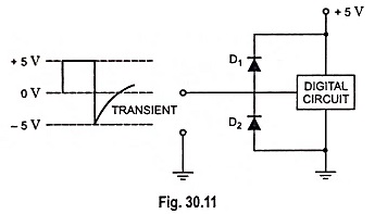
The Diode Clipping Circuit can be used for the protection of different types of circuits e.g., a digital circuit against transients which may cause considerable damage. The arrangement is shown in Fig. 30.11. When a transient takes place on the input line, as shown in Fig. 30.11, diode D2 gets forward biased and starts conducting. Thus transient is shorted to ground and the circuit is protected from damage due to transient.