What is Low Frequency Compensation?
The coupling or blocking capacitor tilts the amplifier response for step input. In Fig. 16.28, if a high value of resistance Rd is added in series with RC which connects to the supply voltage and bypass this resistor to ground with a large capacitance Cd, the tilt in the output waveform can be compensated. These components Rd and Cd are used with a multistage amplifier as a decoupling filter to reduce the interaction between stages due to use of common power supply. The same decoupling network compensates for the low frequency compensation due to Cb. Thus at high frequencies (in the mid band region) Cd acts as a short-circuit across Rd, and the amplifier gain is determined by Ry.
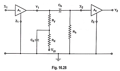
At low frequencies Cd results in a large reactance and the effective output-circuit resistance is, therefore, increased by a value of Ry + Rd. This increase in amplification tends to compensate for the loss in the output due to the attenuation caused by reactance Cb, which increases with the reduction in frequency.
For perfect compensation
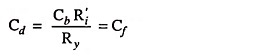
It is seen that the perfect low frequency compensation corresponds to the case where the two branches of the circuit shown in Fig. 16.29 have the same time constant. The capacitance Cf for perfect compensation may be quite large. For example for a transistor for which R′i is of the same order of magnitude as Ry = RC; Cf ≈ Cb ≈ 50 μF
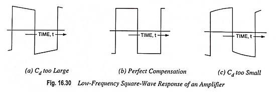
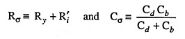
It is to be noted that if a square-wave was to be applied to the amplifier for testing purposes, we would normally select the half period of the square-wave to be approximately 0.1 Rσ Cσ where
In this case the input square wave would, after transmission through the amplifier, have the appearance of the curves shown in Fig. 16.30.