Depletion Type MOSFET – Construction, Operation and Characteristics:
As we know already that when the gate is biased negative w.r.t. the source in an N-channel JFET, the depletion-region widths are increased. The increase in the depletion regions reduces the channel thickness, which increases its resistance. The net result is that drain current ID is reduced.
If the polarity of VGG were reversed so as to apply a positive bias to the gate w.r.t. source, the P-N junctions between the gate and the channel would then be forward biased. Since a forward bias reduces the width of a depletion region, the thickness of channel would increase with a corresponding decrease in channel resistance. As a result, drain current ID would increase beyond the JFET’s IDSS value.
The normal operation of a JFET is in its depletion mode of operation. However, as discussed above, it is also possible to enhance the conductivity of the JFET channel. However, the forward bias of the silicon P-N junction is usually restricted to a maximum of 0.5 V (more conservative limit is 0.2 V) so as to limit the gate current.
As we know already that, the greater the ID is compared to IDSS, the greater the transconductance gm will be. We have seen already that the voltage gain is directly proportional to gm. So, in general, the higher the gm, the better it is. This is one of the advantages of being able to enhance the channel.
As its name suggests, the depletion type MOSFET (DE-MOSFET) was developed to be used in either or both the depletion and enhancement modes.
Construction of Depletion Type MOSFET:
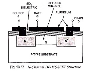
Figure 13.67 shows the construction of an N-channel DE-MOSFET. It consists of a lightly doped P-type substrate into which two blocks of heavily doped N-type material are diffused forming the source and drain. An N-channel is formed by diffusion between the source and drain. The type of impurity for the channel is the same as for the source and drain. Now a thin layer of SiO2 dielectric is grown over the entire surface and holes are cut through the SiO2 (silicon dioxide) layer to make contact with the N-type blocks (Source and Drain). Metal is deposited through the holes to provide drain and source terminals, and on the surface area between drain and source, a metal plate is deposited. This layer constitutes the gate. SiO2 layer results in an extremely high input impedance of the order of 1010 to 1015 Ω for this device. The chip area of a MOSFET is typically 0.003 μm2 or less which is about only 5% of the area required by a BJT.
A P-channel DE-MOSFET is constructed like an N-channel DE-MOSFET, starting with an N-type substrate and diffusing P-type drain and source blocks and connecting them internally by a P-dopped channel region.
In some cases the substrate is internally connected to the source terminal S and in others an additional terminal labelled SS is provided resulting in a four terminal device.
Silicon dioxide (SiO2) is a type of insulator referred to as a dielectric, which develops opposing (as indicated by the prefix di-) electric fields within the dielectric when exposed to an externally applied field. The fact that the SiO2 layer is an insulating layer means that there is no direct electrical connection between the gate terminal G and the channel of a MOSFET. It is the insulating layer of SiO2 in the MOSFET construction that accounts for the very desirable high input impedance of the device.
In fact, the input resistance of a MOSFET is usually much higher than that of a typically JFET, even though the input impedance of most JFETs is sufficiently high for applications. Because of very high input impedance, the gate current IG is essentially zero for dc-biased configurations.
Operation of Depletion Type MOSFET:
It is obvious from Fig. 13.67 that there is no P-N junction between gate and channel. Here the diffused channel N, the insulating dielectric SiO2 layer and the metal layer of the gate forms a parallel plate capacitor. DE-MOSFET can be operated with either a positive or a negative gate. When gate is positive with respect to the source it operates in the enhancement—or E-mode and when the gate is negative w.r.t. the source, as illustrated in Fig. 13.68, it operates in depletion-mode.
When the drain is made +ve with respect to source, a drain current will flow, even with zero gate potential and the MOSFET is said to be operating in E-mode. In this mode of operation gate attracts the –ve charge carriers from the P-substrate to the N-channel and thus reduces the channel resistance and increases the drain current. The more positive the gate is made, the more drain current flows.
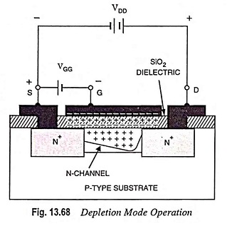
On the other hand when the gate is made –ve with respect to the substrate, the gate repells some of the –ve charge carriers out of the N-channel. This creates a depletion region in the channel, as illustrated in Fig. 13.68, and, therefore, increases the channel resistance and reduces the drain current. The more –ve the gate, the less the drain current. In this mode of operation the device is referred to as a Depletion Type MOSFET. Here too much negative gate voltage can pinch off the channel. Thus operation is similar to that of JFET.
Characteristics:
Typical drain characteristics, for various levels of gate-source voltage, of an N-channel MOSFET are shown in Fig. 13.69. The upper curves are for positive VGS and the lower curves are for negative VGS. The bottom drain curve is for VGS = VGS (OFF). For a specified drain-source voltage VDS, VGS (OFF) is the gate-source voltage at which drain current reduces to a certain specified negligibly small value, as shown in Fig. 13.69. This voltage corresponds to the pinch-off voltage VP of JFET. For VGS between VGS (OFF) and zero, the device operates in depletion-mode while for VGS exceeding zero the device operates in enhancement mode.
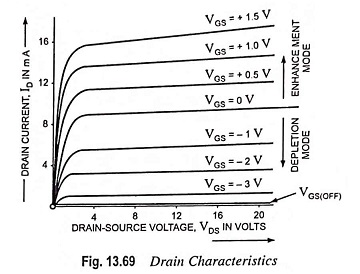
These drain curves again display an ohmic region, a constant current source region and a cutoff region. MOSFET has two major applications: a constant current source and a voltage variable resistor.
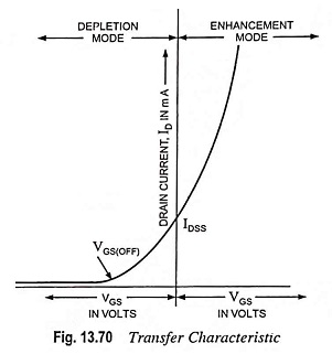
The transfer (or transconductance) characteristic for an N-channel DE-MOSFET is shown in Fig. 13.70. IDSS is the drain current with a shorted gate. Since the curve extends to the right of the origin, IDSS is no longer the maximum possible drain current. Mathematically, the curve is still part of a parabola and the same square-law relation exists as with a JFET. In fact, the Depletion Type MOSFET has a drain current given by the same transconductance equation. Furthermore, it has the same equivalent circuits as a JFET. Because of this, the analysis of a Depletion Type MOSFET circuit is almost identical to that of a JFET circuit. The only difference is the analysis for a positive gate, but even here the same basic formulas are used to determine the drain current ID, gate-source voltage VGS etc.
The foregoing discussion is applicable in principle also to the P-channel DE-MOSFET. For such a device the sign of all currents and voltages in the characteristics [Figs. 13.69 and 13.70] must be reversed.
Schematic Symbols:
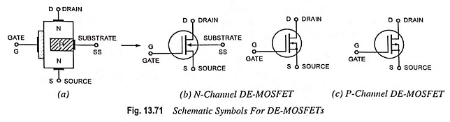
Figure 13.71 (a) shows the schematic symbol for a DE-MOSFET. Just to the right of the gate is the thin vertical line representing the channel. The drain lead comes out from the top of the channel and the source lead connects to the bottom. The arrow is on the P-substrate and points to the N-material. In some applications, a voltage can be applied to the substrate for added control of drain current. For this reason, some DE-MOSFETs have four terminal leads. But in most applications, the substrate is connected to the source. Usually the substrate is connected to the source internally by the manufacturer. This results in a three terminal device whose schematic symbol is shown in Fig. 13.71(b).
Schematic symbol for a three terminal P-channel DE-MOSFET device is shown in Fig. 13.71(c). The schematic symbol of a P-channel DE-MOSFET is similar to that of an N-channel DE-MOSFET, except that the arrow points outward.
DE-MOSFET Amplifiers:
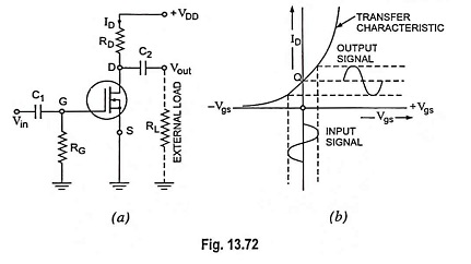
DE-MOSFET can be operated either with positive or negative gate, so its operating or quiescent point can be set at VGS = 0 V, as illustrated in Fig. 13.72(b). In Fig. 13.72(a) the gate G is at ground potential for dc since ac signal source appears to be short circuited for dc and sets Q-point at VGS = 0 V. The ac input signal causes the gate-source voltage Vgs to vary above and below zero developing drain current ID and drain voltage Vout. The biasing circuit given in Fig. 13.72(a) has Vgs = 0 V, ID = IDSS and dc drain voltage
![]()
The zero bias of Fig. 13.72(a) is unique with depletion-mode MOSFETs. Although any of the JFET biasing method will work with a Depletion Type MOSFET, the zero-bias method shown in Fig. 13.72(a) is preferred as it does the job simply and adequately.
After biasing the Depletion Type MOSFET to a Q-point, it can amplify small signals. The JFET formulas for voltage gain can be applied directly to a MOSFET amplifier. But like the JFET, the depletion-mode MOSFET has a relatively low voltage gain. MOSFETs have excellent low-noise properties, a definite advantage for any stage near the front end of a system where the signal is weak, such as a TV receiver. As with a JFET, the transconductance gm in case of MOSFET can be controlled by varying the gate-source voltage Vgs. Due to the fact that a DE-MOSFET is normally an on device, it is also possible to use self-bias by adding a source resistor. The operation becomes the same as a self-biased JFET circuit.
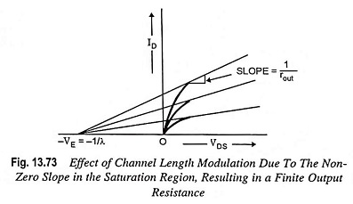
Effect of Channel Length Modulation:
In actual MOSFET characteristic, shown in Fig. 13.73, a nonzero slope exists beyond the saturation point. For the saturation region i.e. (VDS > VDS(sat)), the effective channel length decreases and this phenomenon is known as channel length modulation. For an N-channel device, the slope of the curve in the saturation region may be expressed by using the drain current ID given by
![]()
where λ is a positive quantity termed as the channel length modulation parameter and λ-1 is analogous to the Early voltage in BJTs, KN is the conduction parameter and VGST is the threshold gate voltage. The curves are extended so that the intercept at a point ID = 0, VDS = -VE which means that VE = 1/λ.
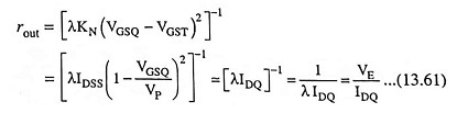
The output resistance due to the channel length modulation is given by
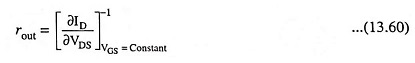
The output resistance can be determined at the Q-point by
The output resistance is an important factor in the analysis of small signal equivalent circuit of MOSFET.
Temperature Effects: The threshold voltage and conduction parameters are the functions of temperature. The magnitude of threshold voltage falls with the temperature and therefore, the drain current ID increases with temperature at a given VGS. The conduction parameter is directly proportional to mobility (μe or μh) of the carriers, which increases with the decrease in temperature. Here the temperature dependent of mobility is larger than that of the threshold voltage. Thus the net effect of decrease in drain current at a given VGS due to increase in temperature provides a negative feedback condition and hence the stability for a power MOSFET.