What is Real Diode?
As already mentioned, an actual diode neither behaves as a perfect conductor when forward biased nor as a perfect insulator when reverse biased.
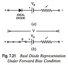
When a diode is forward biased, it will not conduct till the potential barrier V0 (0.7 V for Si and 0.3 V for Ge) at the junction is overcome. When the applied voltage exceeds the potential barrier V0, the diode starts conducting. The forward current, I flowing through the diode causes a voltage drop in its internal resistance r’. Thus the voltage V applied across the diode is to overcome (i) the potential barrier V0 and (ii) internal drop Ir′.
![]()
Hence, a real diodes may be considered as equivalent to an ideal diode in series with a barrier potential of V0 volts and a forward bias ac resistance r’, as illustrated in Fig. 7.21 (a). The equivalent circuit of a real diodes under forward bias condition is shown in Fig. 7.21 (b). This circuit shows that a real diodes still acts as a switch when forward biased but the voltage required to operate this switch is V given by Eq. (7.33).
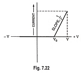
Voltage-current characteristic of a real diodes under forward bias condition is shown in Fig. 7.22 which follows the Eq. (7.33). Here, the reciprocal of the slope of this characteristic represents the ac or dynamic resistance r’ of the diode.
For large signal sources whose voltage is much greater than the diode barrier potential V0 (or knee voltage Vk), forward current I would be large and the ac or dynamic resistance r’ of the diode will be equal to bulk resistance rB of the diode as explained in Fig. 7.11.
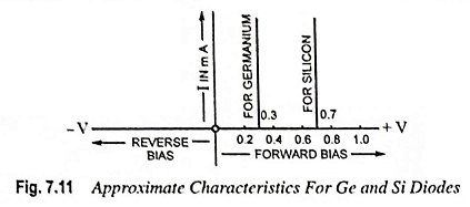
For small signal sources whose voltage is much smaller than V0 or Vk, forward current I would be small and the ac or dynamic resistance of r’ of the diode will be equal to apparent forward or junction resistance r given by Eq. (7.32b) because for smaller values of forward current rB is negligible.
![]()
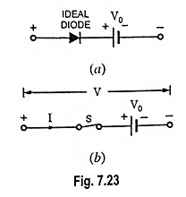
For most applications, the ac or dynamic resistance r’ of a diode can be neglected, being very small as compared to other elements and the real diodes can be represented as shown in Fig. 7.23. The V-I characteristics for a real diodes, neglecting its dynamic resistance become as illustrated in Fig. 7.11.
An actual or real diodes does not behave as a perfect insulator when reverse biased. As already explained in Fig. 7.11, the reverse resistance of silicon and germanium diodes is quite large compared to the forward resistance. It may he of the order of many thousands of mega ohms. Hence an actual diode in the reverse bias condition can be thought of as equivalent to a resistor of high resistance.
The above discussion would be true only in case of small frequency signals. For large frequency signals the capacitive effects would have to be taken into account.
Unilateral diodes can be used for rectification of alternating currents, wave shaping of ac signals and many other applications. Wave shaping involves alteration of ac signals by passing only certain portions of the signal while blocking other portions.
Junction diodes designed for use as rectifiers must have volt-ampere characteristics close to those of an ideal diode. The reverse current should be negligible and forward current should exhibit little voltage dependence. The reverse breakdown voltage should be large and the offset or barrier potential V0 in forward direction should be small. No diode can offer all these properties.
The requirements for good rectifier junctions are :
- Band Gap. A rectifier with a wide band gap material can operate at higher temperatures as thermal excitation of electron-hole pairs (EHPs) is reduced by the increased band gap. Temperature effects are critical in rectifiers, which carry large currents in forward direction and are thereby subjected to appreciable heating. On the other hand, the contact potential and offset voltage generally increase with EG. Silicon is preferred over germanium because of its wider band gap, lower leakage current, higher breakdown potential and also convenient fabrication properties.
- Doping Concentration. This affects the avalanche breakdown voltage, the contact potential, and the series resistance of the diode.
- Physical Geometry. Limitations on the diode area lead to difficulties in uniform starting material and junction processing over large areas. Premature reverse breakdown can sometimes occur. This effect can be controlled by beveling the edge or by diffusing a guard ring to isolate the junction from the edge of the sample.
Piecewise Linear Diode Characteristic
A large-signal approximation which usually leads to a sufficiently accurate engineering solution is the piecewise linear representation. For instance, the piecewise linear approximation for a semiconductor diode is given in Fig. 7.22. The break point is not at the origin, and therefore, V0 (or Vγ) is also known as the offset, or threshold, voltage. The diode behaves like an open circuit when the applied voltage is less than potential barrier V0, and has a constant incremental resistance r′ = dV/dI when applied voltage exceeds potential barrier or threshold voltage. The equivalent circuit for this linear approximation is a constant voltage source in series with a resistor [Fig. 7.21 (b)]. This method models the diode with segments of straight lines : thus the name piecewise linear model.
Note:
- The ideal diode is the first approximation of a diode.
- Visualization of silicon diode as a switch in series with a keen voltage of 0.7 V [Fig. 7.23(b)] is the second approximation. As the voltage across the silicon diode exceeds 0.7 V, the switch closes.
- Visualization of silicon diode as a switch in series with a knee voltage and internal resistance γ′, as shown in Fig. 7.21(b). This is the third approximation.