Dual Input Balanced Output Differential Amplifier:
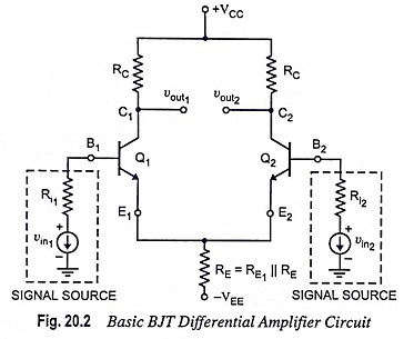
The dual input balanced output differential amplifier configuration is shown in Fig. 20.2. In the given circuit two input signals vin1 and vin2 are applied to the bases B1 and B2 of transistors Q1 and Q2. The differential input under amplification is the difference of the two input signals vin1 and vin2 and denoted by vd. The output in this configuration is balanced as it is measured between the two collectors C1 and C2, which are at the same dc potential w.r.t. ground.
1. DC Analysis:
DC analysis of a differential amplifier circuit is done for determination of operating points (ICQ and VCEQ) when no signal is applied (i.e., vin1 = vin2 = 0). For dc analysis we require a dc equivalent circuit of the differential amplifier. The dc equivalent circuit of the circuit given in Fig. 20.2 is shown in Fig. 20.3 which is obtained by setting vin1 = vin2 = 0. Since, both the transistors Q1 and Q2 are identical (matched pair) and also the passive loads (RC1 = RC2 = RC) are the same, we are to determine Q-point for transistor Q1 only. The same Q-point can be used for transistor Q2 also.
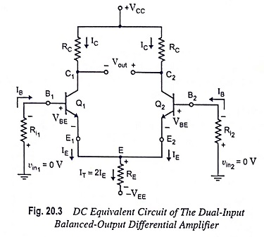
Applying Kirchhoff’s voltage law to the base-emitter loop of the transistor Q1 [Fig. 20.3].
and base current,
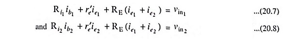
Applying Kirchhoff’s current law at node E, we have
![]()
Substituting IT = 2IE from Eq. (20.3) and IB = IE/βdc from Eq.(20.2) in Eq. (20.1), we have
where VBE = 0.7 V for silicon transistors and VBE = 0.3 V for germanium transistors.
Usually, Ri/βdc << 2RE and , therefore, Eq. (20.4) can be rewritten as

From above Eq. (20.5), we see that the value of RE fixes the emitter current in transistors Q1 and Q2 for a given value of –VEE. Thus, the desired value of the emitter dc bias current for a given value of –VEE can be obtained by selecting emitter resistance RE of a proper value. Thus, we see that emitter current in transistors Q1 and Q2 is independent of collector resistance RC.
The voltage at the emitter of transistor Q1 is approximately equal to –VBE if the voltage drop across Ri is assumed to be negligibly small. Knowing the value of emitter current IE from Eq. (20.5), the voltage at the collector, VC can be determined from the following equation
![]()
and collector-to-emitter voltage,

Hence for both transistors ICQ and VCEQ can be determined by using Eqs. (20.4) and (20.6) respectively, because at the Q-point, IE = ICQ and VCE = VCEQ.
The noteworthy point is that the dc analysis Eqs. (20.4) and (20.6) are applicable to all four differential amplifier configurations as long as the biasing arrangement (as discussed above) is the same for each of them.
2. AC Analysis:
The expressions for the differential voltage gain Ad, common mode gain Acm and the input resistance Rin can be derived from ac analysis of the dual input balanced output differential amplifier.
For ac analysis of the differential amplifier shown in Fig. 20.2, the dc voltages +VCC and –VEE are set at zero and small signal T-equivalent models are substituted for the transistors Q1 and Q2, as shown in Fig. 20.4 (a).
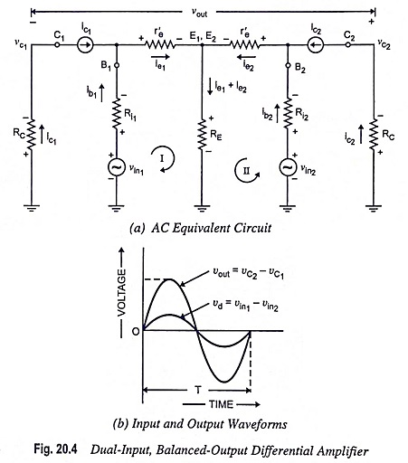
The noteworthy points about the circuit given in Fig. 20.4(a) are as follows:
- Emitter currents IE1 and IE2 are equal, so r′e1 = r′e2. That is why, the dynamic or ac emitter resistance of transistors Q1 and Q2 is simply denoted by r′e.
- The voltage across each collector resistor is shown to have a phase difference of 180° (i.e., in phase opposition) with respect to input voltages vin1 and vin2. The polarity assignment is according to the CE configuration, the differential amplifier being basically constructed in CE configuration using two identical CE circuits.
- The polarity of the output voltage vout indicates that the voltage at collector C2 is assumed to be more positive with respect to that of collector C1, even though both of them are negative w.r.t. ground.
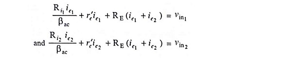
(i) Voltage Gain: Applying KVL to loops I and II of the circuit given in Fig. 20.4 (a), we have
Substituting ib1 = ie1/βac and ib2 = ie2/βac in above equations, we have
Usually Ri1/βac and Ri2/βac, being very small, are neglected and, therefore, the above equations become as follows:

Solving above Eqs. (20.9) and (20.10) for currents ie1 and ie2, we have
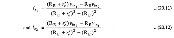
The output voltage is given by
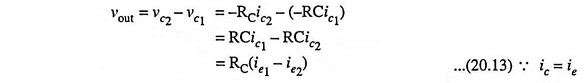
Substituting the values of ie1 and ie2 from Eqs. (20.11) and (20.12) in above equation, we have
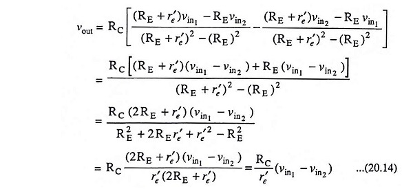
Above Eq. (20.14) shows that a differential amplifier amplifies the difference of two input signals as expected. The input and output waveforms of the dual input balanced output differential amplifier are depicted in Fig. 20.4 (b).
By defining vin1 – vin2 = vd as the difference in input voltages, the voltage gain equation for the dual input balanced output differential amplifier is given by

Above Eq. (20.15) reveals that the voltage-gain equation for the differential amplifier is independent of emitter resistance RE and this equation is identical to the voltage-gain equation of the CE amplifier.
(ii) Differential Input Resistance: Differential input resistance seen from the signal source is defined as the equivalent resistance that would be measured at either input terminals with the other terminal grounded. Usually source resistances Ri1 and Ri2 are negligibly small and, therefore, will be ignored in the derivation of input resistances Rin1 and Rin2 seen seen from the input signal sources vin1 and vin2 respectively.
The input resistance Rin1 seen from the input signal source vin1 is determined by setting signal source vin2 at zero and is expressed in equation form as

Substituting the value of ie1 from Eq. (20.11) in above equation, we have
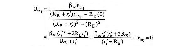
Usually, RE >> r’e which implies that (r′e + 2RE) ≡ 2RE and (r′e + RE) ≡ RE and, therefore, above equation becomes

Similarly, the input resistance Rin2 seen from the input signal vin2 is determined with the signal source vin1 set at zero and is expressed in equation form as

Substituting the value of ie2 from Eq. (20.12) in above equation, we have

However, (2RE + r′) ≡ 2RE and (RE + re) = RE since r′e << RE and, therefore, the above equation for Rin2 becomes as

(iii) Output Resistance: The output resistance may be defined as the equivalent resistance measured at either output terminal with respect to ground. Hence, the output resistance Rout1 measured between collector C1 and ground is equal to collector resistance RC [Fig. 20.4 (a)] i.e., Rout1 = RC.
Similarly, the output resistance Rout2 measured between collector C2 and ground is equal to collector resistance RC i.e., Rout1 = RC.
![]()
3. Noninverting and Inverting Inputs:
In the differential amplifier circuit shown in Fig. 20.2, the input voltage vin1 is referred to as a noninverting input as a positive voltage vin1 acting alone provides a positive output voltage. This is obvious from voltage-gain Eq. (20.14). Similarly, the positive voltage vin2 acting alone produces a negative output voltage, and therefore, vin2 is referred to as a inverting input [Eq. (20.14)]. Consequently, the base terminal B1 to which vin1 is impressed is known as the noninverting input terminal, and the base terminal to which vin2 is applied is known as the inverting input terminal. Noninverting input terminal is marked with plus (+) sign and inverting input terminal is marked with minus (-) sign.
4. Common-Mode Voltage Gain:
If in-phase signals vin are applied to each base of the differential amplifier, as depicted in Fig. 20.5(a), the input signal is referred to as common-mode signal vcm. Ideally, there will be no ac output voltage with a common-mode input signal because the voltage between the bases is zero. However, due to imperfections within the differential amplifier there will be a small ac output voltage.
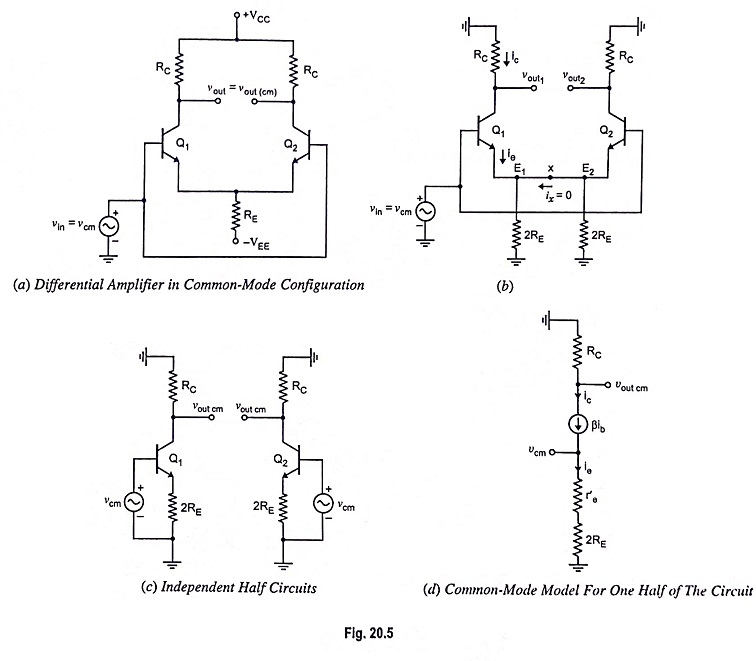
In Fig. 20.5(a) equal voltages are applied to the two inputs. A differential amplifier is never used deliberately in this way because the output voltage would be ideally zero. Then what is the need of discussing such a circuit. This is because most static, interference, and other kinds of undesirable pickups are common mode signals.
Because the differential amplifier is a symmetrical circuit, emitter resistance RE can be split into two parallel resistors, as illustrated in Fig. 20.5 (b). Because of symmetry of the circuit, lead connecting the two emitters E1 and E2 carries no current i.e., ix = 0 because emitters E1 and E2 are at the same potential.
With ix = 0, connection between two emitters can be eliminated and the resulting independent half circuits are shown in Fig. 20.5 (c). The common-mode behavior can be determined from only one-half of the circuit.
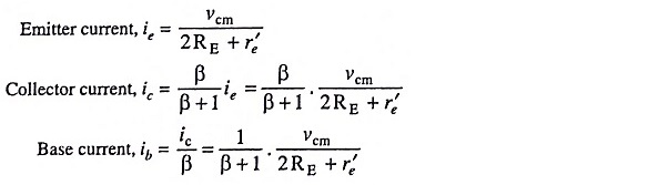
Using r-parameters, the common model for one half of the circuit is depicted in Fig. 20.5 (d).
Referring to Fig. 20.5 (d), we have

The common-mode output voltage is, therefore,

The common-mode voltage gain Acm is, therefore,

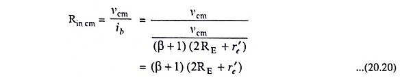
5. Common-Mode Input Resistance Rin cm
Common-mode input resistance is obtained as under:
Common mode input resistance,
6. Common-Mode Rejection Ratio (CMRR)
Having defined differential voltage gain Ad and common mode voltage gain Acm, a value of the common-mode rejection ratio (CMRR) can be calculated from the following equation

i.e., CMRR may be defined as the ratio of differential voltage gain to common-mode voltage gain.
If a differential amplifier is perfect, CMRR would be infinite because in that case common-mode voltage gain Acm would be zero.
The value of CMRR can also be expressed in logarithmic terms as

Data sheets usually list the values of Ad and CMRR’, but not the value of Acm. However, the value of Acm can be determined from the following equation