MOSFET Construction and Characteristics:
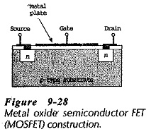
Figure 9-28 shows the MOSFET Construction and Characteristics of a metal oxide semiconductor FET (MOSFET), also known as an insulated gate FET. Starting with a high-resistive p-type substrate, two blocks of heavily-doped n-type material are diffused into the substrate, and then the surface is coated with a layer of silicon dioxide. Holes are cut through the silicon dioxide to make contact with the n-type blocks. Metal is deposited through the holes for source and drain terminals, as illustrated, and a metal plate is deposited on the surface area between drain and source. As will be explained, this plate functions as a gate.
Consider the situation illustrated in Fig. 9-29(a). The drain terminal of the MOSFET is positive with respect to the source, and the gate is open-circuited. The two n-type blocks and the p-type substrate form back-to-back pn-junctions connected by the resistance of the p-type material, as illustrated. The pn-junction close to the drain terminal is reverse biased, so only a very small (reverse leakage) current flows from D to S.
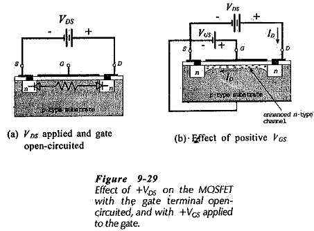
Now assume that the source terminal is connected to the substrate, and that a positive gate voltage is applied, as shown in Fig. 9-29(b). Negative (minority) charge carriers within the substrate are attracted to the (positive) plate that constitutes the gate. These charge carriers (electrons) cannot cross the silicon dioxide to the gate, so they accumulate close to the surface of the substrate, as shown. The minority charge carriers constitute an n-type channel between drain and source, and as the gate-source voltage is made more positive, more electrons are attracted into the channel causing the channel resistance to decrease. A drain current flows along the channel between the D and S terminals, and because the channel resistance is controlled by the gate-source voltage (VGS), the drain current is also controlled by the level of VGS. The channel conductivity is said to be enhanced by the positive gate-source voltage, so the device is known as an enhancement-mode MOSFET, (E-MOSFET).
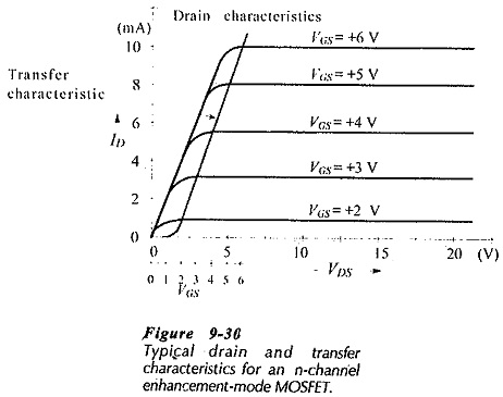
Typical drain and transfer characteristics for an enhancement mode n-channel MOSFET are shown in Fig. 9-30. Note on both characteristics that the drain current increases as the positive gate-source bias voltage is increased. Because the gate of the MOSFET is insulated from the channel, there is no gate-source leakage current, and the device has an extremely high (gate) input resistance; typically 1015 Ω, or greater. Forward transfer admittance values for this type of (low-power) MOSFET typically range from 1 mS (1 mA/V) to a maximum of perhaps 6 mS, which is similar to JFET Yfs values.
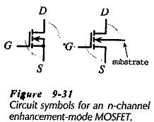
Two graphic symbols for the n-channel E-MOSFET are shown in Fig. 9-31. One symbol shows the source and substrate connected internally, while the other has a separate substrate terminal. The line representing the device channel is broken into three sections, to indicate that the channel does not exist until an appropriate gate voltage is applied. The fact that the device has an insulated gate is illustrated on the symbols by the gate not making direct contact with the channel. The arrowhead points from the p-type substrate to the n-type channel.
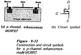
A p-channel E-MOSFET Is constructed by starting with an n-type substrate and diffusing p-type drain and source blocks, as illustrated in Fig. 9-32(a). The device MOSFET Construction and Characteristics are similar to those in Fig. 9-30, except that all voltage polarities and current directions are reversed. The drain-source voltage is negative, and a negative gate-source voltage is required to create the p-type channel. The arrowhead in the circuit symbols are also reversed,[see Fig. 9-32(b)].
Depletion-Enhancement MOSFET:
The device cross-section shown in Fig. 9-33(a) is similar to that for an enhancement-mode MOSFET, except that a lightly-doped n-type channel is included between the drain and source blocks. When a positive drain-source voltage (VDS) is applied, a drain current (ID) flows even when the gate-source voltage (VGS) is zero. If a negative VGS is applied, as shown in Fig. 9-33(b), some of the negative charge carriers are repelled from the gate and driven out of the n-type channel. This creates a depletion region in the channel, as illustrated, causing an increase in channel resistance and a decrease in drain current. The effect is similar to that in an n-channel JFET. Because of the channel depletion regions, the device can be termed a depletion-mode MOSFET.
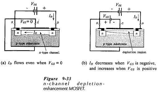
Now consider what occurs when a positive gate-source voltage is applied. Additional n-type charge carriers are attracted from the substrate into the channel, decreasing its resistance and increasing the drain current. So, the depletion-mode MOSFET can also be operated as an enhancement-mode device. Thus, these devices are referred to as depletion-enhancement MOS, or DE-MOS.
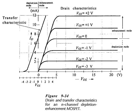
Typical drain and transfer characteristics for a DE-MOSFET are shown in Fig. 9-34. The device operates in the depletion-mode when VGS is negative, and in the enhancement-mode when positive levels of VGS are used.
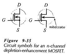
The circuit symbols used for DE-MOSFETs are similar to those already discussed for E-MOSFETs, except that the line representing the channel is made solid to show that a channel is present when VGS = 0, (see Fig. 9-35).
VMOS:
A disadvantage of the MOSFET Construction and Characteristics types already discussed is that the minimum channel length depends upon the dimensions of the photographic masks used in the manufacturing process. Shorter channel lengths can be produced by changing the geometry of the MOSFET to create a vertical channel (instead of horizontal). The channel length is then easily determined by the diffusion process. The shorter channel results in lower resistance, greater power dissipation, higher frequency response, and larger forward transfer admittance values than are possible with other MOSFETs.
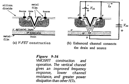
Figure 9-36(a) shows a device referred to as a VMOSFET because of its V-shaped configuration, and because it uses a vertical channel between drain and source. The V-cut penetrates from the surface of the device through n+, p, and n– layers almost to the n+ substrate. The n+ layers are low-resistive, and the n– is a high-resistive region. The silicon dioxide layer covers horizontal surface and the V-cut surface. The gate is a metal film deposited on the silicon dioxide surface in the V-cut. The drain terminal is at the bottom of the n+ substrate, and the source connection is made to the top n+ region and to the p region.
The VFET operates in the enhancement-mode; no channel exists until a positive gate source voltage is applied. An n-type channel is created as shown in Fig. 9-36(b) when VGS is made positive, and a current flows vertically from drain to source.
Some versions of VMOS use a vertical channel, but do not use the V-cut. MOTOROLA currently manufactures devices referred to as TMOS, because the drain current flow tends to be T-shaped.

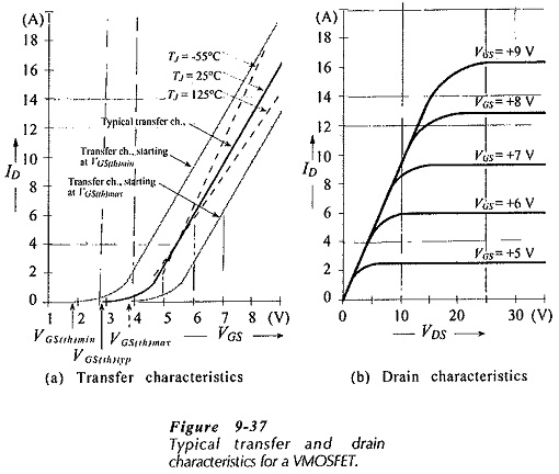
Typical VFET drain and transfer characteristics are shown in Fig. 9-37. It is seen that they are similar to the enhancement-mode device characteristics in Fig. 9-30, although much higher drain current levels are usually involved with a VFET than with other MOSFET Construction and Characteristics. The MOSFET Construction and Characteristics shown are for a device capable of dissipating 40 W.
The VFET transfer characteristic is seen to be approximately linear over most of its length, and it is curved (non-linear) only at the low current levels. For the typical characteristic shown, ID commences at the typical gate threshold voltage (VGS(th)typ), and the slope of the linear portion of the graph is set by the typical gFS value (same as YFS). It should be noted that for a device with a given type number ID might commence at VGS(th)min or VGS(th)max and that the slope of the characteristic depends upon the actual gFS for the device. Temperature changes can also have a serious effect on the characteristics, as shown by the dashed lines.
The graphic symbols used for VMOS devices are the same as for other enhancement-mode MOSFET Construction and Characteristics. However, a parasitic pn-junction is present between the p and n layers in a VFET, and this must not be allowed to become forward biased. So, the diode is usually shown on the device symbol, (see Fig. 9-38).
Handling MOSFETs:
Figure 9-40 shows the kind of label normally found on packages containing MOSFETs. This indicates that the devices can be very easily destroyed by electrostatic discharge (ESD); that is, discharge of static electricity that accumulates on individuals or objects. Usually, the very thin layer of silicon dioxide at the gate breaks down when an excessive gate-source voltage is applied. Special precautions are necessary to protect MOSFETs from ESD:
- Always store MOSFETs in closed conductive containers. Usually they are packaged with the terminals inserted into conducting foam rubber.
- Use a work station with a grounded anti-static bench-top pad and a grounded anti-static floor pad.
- Wear anti-static clothing and grounded wrist bands.
- Use a soldering iron with a grounded tip.
- Avoid touching the device terminals.
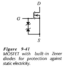
Some MOSFETs have built-in protection against static electricity. Back-to-back series-connected Zener diodes are located between the gate and source terminals, as illustrated in Fig. 9-41. When the gate-source voltage is high enough to reverse bias one of the diodes into breakdown, the other diode is forward biased. Thus, the gate-source voltage cannot exceed ±(VZ + VF).