Energy Band Diagram of Semiconductors, Insulators and Metals:
Energy Band Diagram of Semiconductors, Insulators and Metals – As discussed earlier, the electrons of an isolated atom are acted upon only by the forces within that atom. However, when atoms are brought together, as in a solid, the electrons come under the influence of forces from other atoms. Under these conditions, the energy levels that may be occupied by electrons merge into bands of energy levels. Within any given material there are two distinct energy bands in which electrons may exist. These two energy bands are valence energy band (or valence band) and conduction energy band (or conduction band) and are separated by an energy gap in which no electron can normally exist, as illustrated in Fig. 6.4. This energy gap is termed as forbidden energy gap (or forbidden gap).
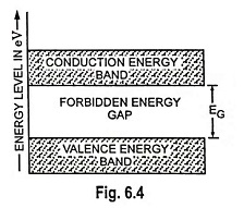
The energy band of interest is the highest energy band or valence band. If a sufficient amount of energy is given to an electron in the valence band, the electron is freed from the atomic structure. Such an electron is said to possess enough energy to be in the conduction band, where it can take part in electric current flow. Free electrons (electrons in conduction band) can move readily under the influence of an external field. Electrons in the valence band are usually in normal orbit around a nucleus. Normally, electrons do not orbit in the forbidden region, which separates the conduction and valence bands, as illustrated in Fig. 6.4.
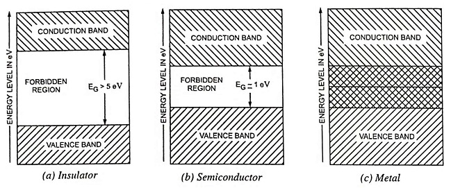
For any given material, the forbidden energy gap may be large, small or non-existent. The distinction between conductors, insulators and semiconductors is largely concerned with the relative widths of the forbidden energy gaps. As illustrated in Figs. 6.5 (a), (b) and (c), there is a wide forbidden gap (more than 5 eV) for insulators, narrow forbidden gap (about 1 eV) in case of semiconductors and no forbidden gap in case of conductors.
In case of insulators, there is practically no electron in the conduction band, and the valence band is filled. For an insulator, the valence and conduction bands are so apart (more than 5 eV) that at normal temperature (25°C) the energy which can be supplied to an electron from an applied field is too small to carry a particle from the filled band into the vacant band. Since the electron cannot acquire externally applied energy, conduction is impossible. Only at very high temperature or under high external electric field, an electron can jump the gap. This is called the breakdown of the insulating material.
For semiconductors at a temperature of absolute zero (-273.15°C) the valence band is usually full and there may be no electron in the conduction band. It means that no current can flow in the semiconductors and, therefore, the Energy Band Diagram of Semiconductors behave as insulators at absolute zero temperature. However, in semiconductor materials, both bands are so close (about 1 eV apart) that an electron can be lifted from the valence band to the conduction band by imparting some energy to it. This energy must be more than energy gap EG. If the energy imparted to the electron is less than EG, it cannot be lifted from valence band to conduction band because no permissible energy level exists between the two bands. The energy imparted by the heat at room temperature is sufficient to lift electrons from the valence band to the conduction band. Some electrons do jump the gap and get into the conduction band. Thus, Energy Band Diagram of Semiconductors are capable of conducting some electric current, even at normal ambient temperature.
In case of conducting materials (metals), there is no forbidden gap, and the valence and conduction bands overlap each other, as illustrated in Fig. 6.5 (c). The orbits in the conduction band are very large. An electron in the conduction band experiences almost negligible nuclear attraction. In fact, an electron in the conduction band does not belong to any particular atom. But it moves randomly throughout the solid. This is the reason that electrons in the conduction band are called the free electrons. Due to overlapping of valence and conduction bands, a slight potential difference across the conductor causes the free electrons to constitute electric current.
The noteworthy point in conductors is that, because of absence of forbidden band, there is no structure to create holes and therefore, the total current in conductors is due to flow of electrons alone.