Band Pass Filter Circuit Diagram:
A Band Pass Filter Circuit Diagram designed to pass signals only in a certain band of frequencies while rejecting all signals outside this band. There are basically two types of Band Pass Filter Circuit Diagram,
- Wide band pass
- Narrow band pass
A Band Pass Filter Circuit is defined as a wide band pass if its figure of merit or quality factor Q < 10. While there is no firm dividing line between the two, if Q > 10, the filter is a narrow Band Pass Filter Circuit Diagram. Hence Q is a measure of selectivity meaning the higher the value of Q, the more selective is the filter, or the narrower is the band width. The relationship between Q, 3 db band width and the centre frequency fc is given by
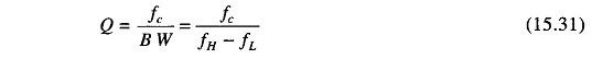
For the wide Band Pass Filter Circuit, the centre frequency can be defined as
![]()
where
- fH = high cutoff frequency
- fL = low cutoff frequency of the wide bandpass
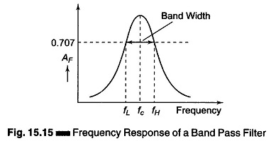
Figure 15.15, shows the frequency response of a Band Pass Filter Circuit Diagram. This type of filter has a maximum output voltage Vmax at one frequency called the resonant frequency, fc. If the frequency is varied away from resonance, the output voltage decreases. There is one frequency above fc and one below fc at which the voltage is 0.707 x Vmax (3 db point). These frequencies are the high and low cutoff frequencies. The band of frequencies between fH and fL is the band width. Therefore the band width is given by BW = fH – fL.
A narrow band filter is one that has a band width of less than 1/10th the resonant frequency (band width < 0.1 fc). A wide band filter has a band width greater than 1/10th the resonant frequency (band width > 0.1 fc).
The ratio of resonant frequency to band width is known as the quality factor Q.
Wide Band Pass Filter:
Band pass can be realized by a number of possible circuits. A wide band pass filter can be formed by simply cascading high pass and low pass section and is generally the choice for simple to design.
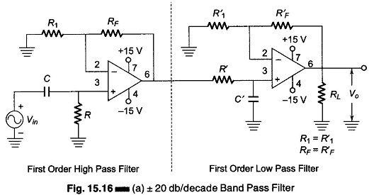
To obtain a ± 20 db/decade band pass filter, a first order high pass filter and a first low pass sections are cascaded, for a ± 40 db/decade band pass filter, second order high pass filter and second order low pass filter are cascaded and so on for higher orders.
In other words, the order of the Band Pass Filter Circuit Diagram depends upon the order of the High pass and Low pass sections.
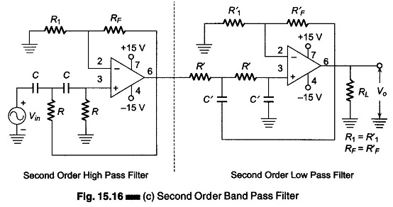
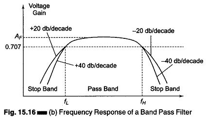
Fig. 15.16(a), shows a circuit of a ± 20 db/decade wide band pass filter, which is composed of a first order high pass and a first order low pass filter. Figure 15.16(b) shows the frequency response.
Figure 15.16(c) shows a circuit of a ± 40 db/decade wide Band Pass Filter Circuit Diagram.
Narrow Band Pass Filter:
The narrow Band Pass Filter Circuit using multiple feedback is shown in Fig. 15.17(a). As shown in this circuit, the filter uses only one opamp. This filter is unique in the following respects.
- It has two feedback paths, which is why it is called a multiple feedback
- The opamp is used in the inverting mode.
Generally a narrow band pass filter is designed for specific values of centre frequency fc and Q, or fc and band width.
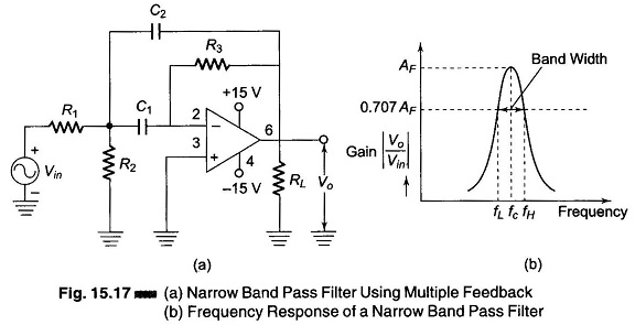
Figure 15.17(b) shows the frequency response of a narrow Band Pass Filter Circuit Diagram.
Mathematical Derivation for Narrow Band Pass Filter:
If we wish to realise a resonant Band Pass Filter Circuit having the narrow band characteristic of a tuned circuit, we have to use a multiple feedback network in conjunction with an opamp as shown in Fig. 15.17 (a).
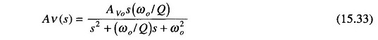
The transfer function of a tuned circuit is given by
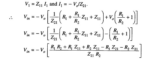
Now let us consider a CR network comprising C1 C2 and R3 as shown in Fig. 15.18.
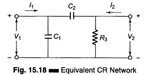
Referring to figure, the z-parameters or impedance parameters are
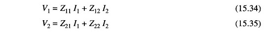
where
- Z11 = input impedance with output open for ac
- Z12 = reverse transfer impedance with input open for ac
- Z21 = forward transfer impedance with output open for ac
- Z22 = output impedance with input open for ac
The equivalent circuit for a narrow Band Pass Filter Circuit is shown in Fig.15.19.
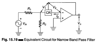
Referring to the figure,

Also due to virtual ground
![]()
But
![]()
The current flowing through R2 is given by

Now consider the mesh Vin R1 R2

But
Simplifying it we have

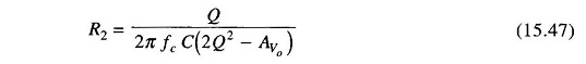
Therefore
We now calculate the values of Z11 and Z21. Referring to the figure for a CR network we have

which reduces to
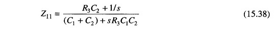
Similarly
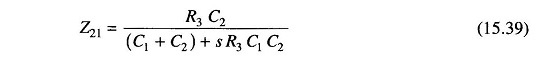
Therefore
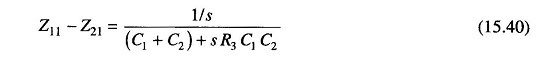
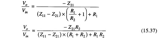
Substituting Eqs (15.38), (15.39) and (15.47) in Eq. (15.37), we get
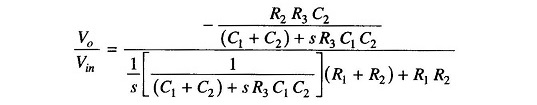
Therefore, gain
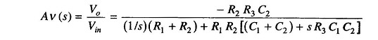
Multiplying the numerator and the denominator by s/R1 R2 R3 C1 C2 we get
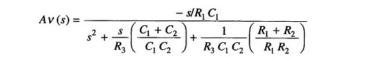
Let
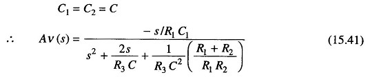
Now comparing Eq. (15.41) with (15.33) we see that
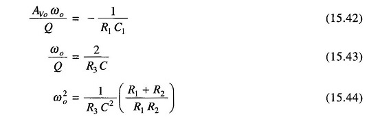
But ωo = 2 πfc where fc = cutoff frequency.
Therefore Eqs (15.42), (15.43) and (15.44) now become
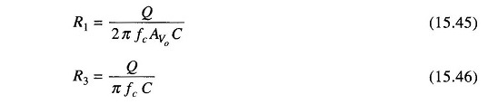
and with slight manipulations with Eq. (15.44) we get
But the gain AVo at fc is given by
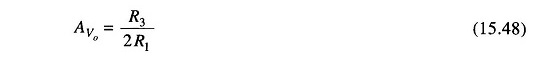
which is derived from a slight manipulation of Eqs (15.45) and (15.46)
Another condition that the gain must satisfy is
![]()
Else we get R2 = 0 which is not possible.