Transistor Current Sweep Circuit:
A simple transistor current sweep circuit is given in Fig. 30.143 (a). In the circuit the transistor is employed as an electronic switch and the inductor in series with the transistor is bridged across the supply voltage VCC. The diode forward resistance and the damping resistance are represented by resistor Rd in Fig. 30.143 (a). The gating waveform depicted in Fig. 30.143 (a) and applied to the transistor base operates between two levels.
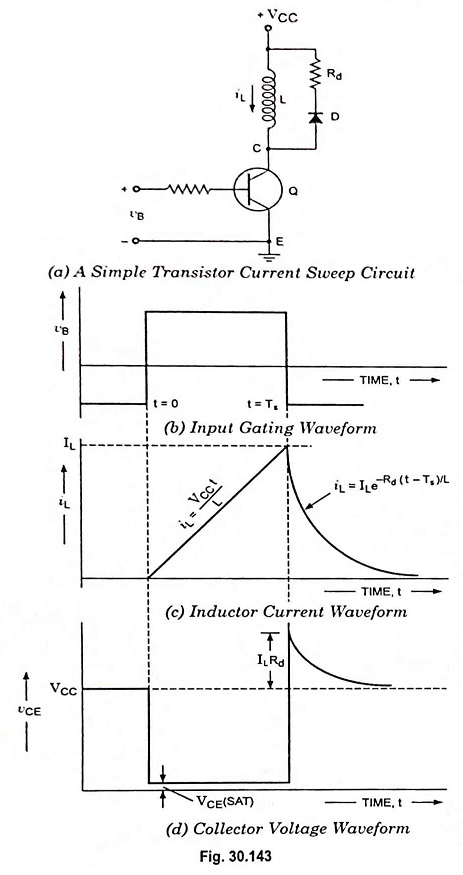
The lower level keeps the transistor Q in cut-off while the upper level drives the transistor into saturation. For t < 0, the input to the base vB is negative (i.e. at its lower level), and, therefore, the transistor is in cut-off. Thus there is no flow of current in transistor, iL = 0 and vCE = VCC. At t = 0, the gate signal goes to its upper level (positive), the transistor conducts and goes into saturation, the collector voltage falls to VCE(sat) and the entire supply VCC acts across the inductor. The inductor current increases linearly with time and is given as
![]()
During this sweep interval the diode D being reverse biased does not conduct. The sweep terminates at t = Ts, when the gating signal drives the transistor to cut-off. The inductor current iL then continues to flow through the diode D and resistor Rd until it decays to zero. This decay is exponential with a time constant τ = L/Rd. This is because the current flowing through the inductor cannot change instantaneously. The inductor current waveform is depicted in Fig. 30.143 (c), where it is indicated that the gate duration Ts is such that the current attains a maximum value IL.
Before the transistor is turned ‘on’, and some time after it has been turned ‘off’ vCE = VCC. When the transistor is ‘on’, the voltage vCE is quite small, being only some tens of millivolts for a germanium unit driven well into saturation. At the moment the transistor is turned “off” a spike of amplitude ILRd appears across the inductor L.
This peak voltage must be limited so that the transistor is below its collector-to-base breakdown voltage. As inductor current Id may well be determined by deflection requirements, there is clearly an upper limit to the size of Rd. The spike decays with the same time constant as does the inductor current. The noteworthy point is that while the spike duration depends on the inductance of L, the spike amplitude does not.
The inductance L normally represents a physical yoke and its resistance RL may not be negligibly small. If RCS is the collector saturation resistance of the transistor, the inductor current increases in accordance with the equation
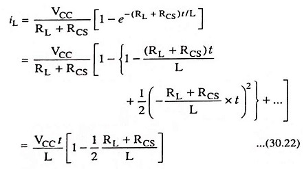
If the current increases linearly to a maximum value, the slope error is given as
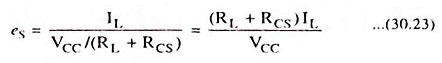
For maintaining linearity, the voltage (RL + RCS)IL across the total circuit resistance must be kept small as compared to the supply voltage VCC.