Explain Transistor Current Components:
The various transistor current components which flow across the forward-biased emitter junction and reverse biased collector junction are indicated in Fig. 10.11. The current flowing into the emitter is referred to as the emitter current and designated as IE. The emitter current IE consists of two constituents (hole current IhE due to crossing of holes from emitter into the base and electron current IeE due to crossing of electrons from base into the emitter).
![]()
In a commercial transistor the emitter is heavily doped and the base is very lightly doped and, therefore, electron current IeE is negligibly small in comparison to hole current IhE. Thus the entire emitter current IE in a P-N-P transistor is due to flow of holes from emitter to the base. It is to be noted that the indicated direction of IE external to the transistor is the conventional current direction.
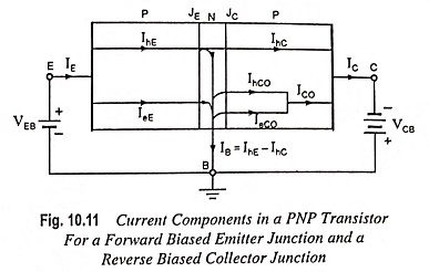
All the holes crossing the emitter junction JE do not reach the collector junction JC because some of them combine with the electrons in the N-type base. If IhC is the hole current at collector junction JC, there must be a bulk recombination current IhE less IhC leaving the base, as shown in Fig. 10.11. In fact electrons enter the base region through the base lead to replenish those electrons which have been lost by recombination with the holes injected into the base across the emitter junction JE. The holes on reaching the collector junction JC cross this junction and enter the collector P-region.
If the emitter were open circuited, IE would have been zero and then IhC also would have been zero. Under these conditions, the base and collector would act as a reverse-biased diode and the collector current IC would be equal to that reverse saturation current ICBO (or simply ICO).
When the emitter circuit is closed i.e., when IE ≠ 0, then from Fig. 10.11
![]()
For a P-N-P transistor, ICO consists of holes moving across junction JC from base region to collector region and electrons crossing junction JC in the opposite direction.
![]()
In the active region operation with emitter junction JE forward biased, the collector current is given as
![]()
where α is the fraction of the total current IE which constitutes IhC.
It is to be noted that the indicated direction of emitter current IE external to the transistor is the conventional current direction. Base current IB and collector current IC are also shown external to the transistor conventional current direction. According to the Kirchhoff s first law total current flowing into the transistor must be equal to the total current flowing out of it. So emitter current IE is equal to the sum of collector and base currents lC and IB.
![]()
Let us now define different parameters which relate the transistor current components discussed above.
Emitter Efficiency: The emitter or injection efficiency denoted by γ is defined as the ratio of current of injected carriers at JE to the total emitter current
![]()
where IhE is the injected hole diffusion current at emitter junction and leE is the injected electron diffusion current at emitter junction.
Transport Factor: Transport factor, denoted by β, is defined as the ratio of injected carrier current reaching JC to the injected carrier current at JE
![]()
Large Signal Current Gain α: The term α has already been defined above. However, α can alternatively be defined from Eq. (10.4). From Eq. (10.4) α may be defined as the ratio of collector current increment from cutoff value (IC = ICO) to lC and the emitter current increment from cutoff value (IE = 0) to IE. Thus, we may write
Term α is called the large signal current gain of a common base transistor. The parameter α is extremely important in transistor theory. It is to be pointed here that α is not constant, but varies with emitter current IE, collector voltage VCB, and the temperature. Typically α lies in the range 0.95 to 0.99.
From Eqs. (10.2) and (10.8) we have
![]()
For an efficient transistor we would like β and γ to be very near unity i.e., the emitter current should be due mostly to holes (γ = 1) and most of the injected holes should eventually participate in the collector current (β ≈ 1).
The product βγ is defined as the factor α, called the current gain ratio, which represents the emitter-to-collector current amplification. There is no real amplification between these currents, since α is lesser than unity. On the other hand, the relation between collector current and base current is more promising for amplification.
DC Current Gain: If ICO is negligibly small in comparison to lC, α approximately equals IC/IE. This is referred to as the dc current gain of the common base (CB) transistor and is denoted by αdc
Thus
![]()
αdc is always positive and less than unity.
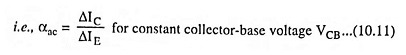
Small Signal Current Gain αac: Small signal current gain αac is defined as the ratio of change in collector current to change in emitter current
αac is always positive but less than unity (very close to unity). It also varies with IE, VCB and temperature.
Generalized Expression For Collector Current: We know that a small reverse current flows across a P-N junction diode due to thermally generated minority carriers that are propelled by the barrier potential. When the junction is reverse biased, this reverse current increases slightly. For moderate reverse-bias voltages, the reverse current attains its saturation value, IS (or I0). Because the collector-base junction of a transistor is reverse biased, there is likewise a reverse current due to thermally generated carriers. Of course this “reverse” current, in the context of a transistor, is in the same direction as the main (collector) current flowing through the device due to the injection of minority carriers into the base. The total collector current is, therefore, the sum of these two transistor current components: the injected minority carriers and the thermally generated minority carriers
![]()
The reverse current ICBO is given by the volt-ampere relationship of equation I = I0(eV/ηVT-1) with I0 replaced by -ICO and V by VC where symbol VC represents the voltage drop across junction JC from the P-side to the N-side and the complete expression for collector current lC may be written as
![]()
If VC is negative and is of large magnitude in comparison with that of VT, Eq. (10.12) reduces to Eq. (10.4).
The physical interpretation of Eq. (10.12) is that the P-N junction diode current crossing the collector junction JC is supplemented by a fraction α of the current IE flowing in the emitter.