Base Modulation Circuit Working Principle:
The circuit for base modulation is shown in Fig. 22.28. The carrier signal from a crystal oscillator is coupled to the base terminal of the amplifier through transformer T1. The modulating signal is applied across resistor R1 through capacitor C1. The capacitor C1 allows only audio frequency ac signal to pass through and blocks the dc components. The modulating signal develops a voltage across R1, which, in turn, alters the quiescent point in the base circuit. With the increase in bias current, the signal at the collector terminal is correspondingly strengthened.
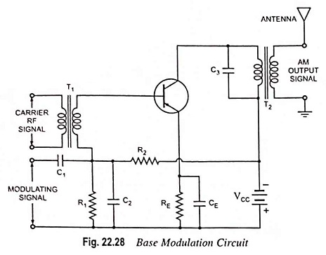
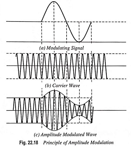
Similarly, as the bias current falls during the reverse part of the cycle of the modulating signal, the output at the collector terminal is also reduced. Consequently, a plot of the collector output will be found to give a variation similar to that shown in Fig. 22.18.
The resistor RE is the self-bias emitter resistor and CE is its bypass capacitor. Also, R2 is a dropping resistor which limits the dc voltage drop across R1, in turn, establishes the initial quiescent base current. Capacitor C2 is a bypass capacitor for the carrier signal in the input circuit. In understanding the operation of this circuit it is helpful to keep in mind the fact that ωm is very small in comparison to ωc.
Hence for any given cycle of the carrier frequency the bias in the base-to-emitter circuit appears to be fixed. The capacitor C3 is selected to provide series resonance with the primary winding of transformer T2. The amplitude-modulated carrier of RF current in primary of transformer T2 induces similar current in the secondary of transformer T2. Thus the amplitude modulated wave is radiated out in the space by transmitting antenna.
Special Features of Base Modulation:
- Power required from this modulator is small in comparison to that of collector modulator.
- Comparatively low power output and poor efficiency. The power output and efficiency suffer because the unmodulated collector current peaks can be only about half as large as in the collector modulated circuit.
- Critical adjustment of the base modulated amplifier.
- High degree of linearity is more difficult to obtain.
Base modulation is used in TV transmission because it needs little power and can meet the power need of large bandwidth.