Avalanche Photodiode – Definition, Basic Structure and Workings:
The avalanche photodiode is similar to the P-N or PIN photodiode except that it is operated at high reverse-bias voltages so that impact ionization occurs, EHPs are created in the space charge region by photon absorption. Also additional EHPs are created by photon generated electrons and holes through impact ionization.
The avalanche photodiode now has a current gain introduced by the avalanche multiplication factor. The current gain-bandwidth product of an avalanche photodiodes can be larger than 100 GHz, so the device can respond to light modulated at microwave frequencies.
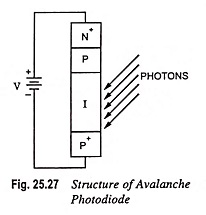
The structure of an avalanche photodiodes is shown in Fig. 25.27. It has four regions N+ and P+ are heavily doped semiconductors and I region is very lightly doped.
For detection of low-level optical signals, it is often desirable to operate the photodiode in the avalanche region of its characteristic.
In the avalanche photodiodes junction must be uniform, and the guard ring is usually employed to ensure against edge breakdown. With proper design a silicon avalanche photodiodes can have high sensitivity to low-level optical signals, and the response time is in the neighborhood of 1 ns. These devices are particularly useful in fibre optic communication systems.