What is Schottky Diode? – Definition, Symbols and Construction:
At lower frequencies, an ordinary diode can easily turn off when the bias changes from forward to reverse. But with the increase in frequency the diode reaches a point where it cannot turn off fast enough to prevent noticeable current during part of the reverse half cycle. The effect is called the charge storage. It restricts the useful frequency of ordinary rectifier diode. How does it happen. it is explained below :
When a diode is forward biased, some of the carriers in the depletion region have not yet recombined. If the diode is suddenly reverse biased, the carriers can flow in the reverse for a while. The greater the lifetime, the longer these charges can contribute to reverse current.
The reverse recovery time is so short in small-signal diodes that its effect cannot be noticed at frequencies below 10 MHz or so. It becomes very important well above 10 MHz.
The solution is a special-purpose device called a Schottky diode. Such a diode has no depletion layer eliminating the stored charges at the junction. Because of lack of charge storage the Schottky diode can switch off faster than an ordinary diode. In fact, a Schottky diode can easily rectify frequencies exceeding 300 MHz.
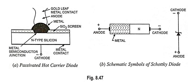
Its construction is very different from the normal P-N junction in that a metal semiconductor junction is developed, as illustrated in Fig. 8.47 (a). On one side of the junction a metal (such as gold, silver, platinum, molybdenum, chrome or tungsten) is used and on the other side of the junction N-type doped silicon (but gallium is often used, especially at high frequencies) is used. Different construction techniques result in a different set of characteristics for the device, such as increased frequency range, lower forward bias, and so on. In general, Schottky diode construction results in a more uniform junction region and increased ruggedness compared to a point contact diode—its main rival.
In both materials, the electrons are the majority carriers. In the metal, the level of minority carriers (holes) is insignificant. When the diode is unbiased, electrons on the N-side have low energy levels than electrons in the metal and so the electrons cannot cross the junction barrier, called the Schottky barrier. But when the diode is forward biased, the electrons on the N-side gain enough energy to cross the junction and enter the metal. Since these electrons plunge into the metal with very large energy, they are usually called the hot carriers and the diode is called the hot-carrier diode.
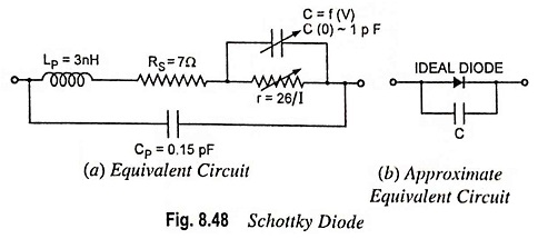
The equivalent circuit for the device (with typical values) is given in Fig. 8.48 (a). The inductance LP and capacitance CP are the package values, and RS is the body (ohmic) series resistance of the diode. The r is the diode resistance and C is the junction capacitance. For many applications, an approximate equivalent circuit, simply including an ideal diode in parallel with the junction capacitance C, illustrated in Fig. 8.48 (b), is used.
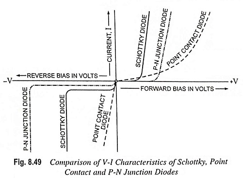
Schottky diode possesses two unique features over an ordinary P-N junction diode viz. (i) It is a unipolar device because of absence of minority carriers in reverse direction (no significant current from metal to the semiconductor in reverse-biased condition), while P-N junction diode is a bipolar device as it has both electrons and holes as majority carriers. (ii) Because of absence of holes in the metal, there is no depletion layer or stored charges to worry about. So Schottky diode can switch off faster than a bipolar diode. Because of larger contact area between semiconductor and metal its forward resistance is lower (i.e., noise is comparatively lower). The Schottky diode also has a lower barrier potential (about 0.2-0.25 V) where normal silicon P-N junction diode has a barrier potential of 0.7 V. This makes it more efficient in high power applications than silicon rectifiers. However, Schottky diode do exhibit higher leakage currents and lower reverse breakdown voltages. Consequently, they are only used when reverse recovery time or efficiency are the main concerns.
A comparison of V-I characteristics of Schottky, point contact and P-N junction diodes is given in Fig. 8.49.