Point Contact Diode Construction and Working:
The point contact diode is basically constructed by touching a metallic whisker to an exposed surface of an N-type semiconductor substrate. The semiconductor used in the point contact diode may be either of germanium or of silicon. However, germanium is preferred over silicon because of its higher carrier mobility. The schematic structure of a point contact diode is shown in Fig. 8.44 (a). It consists of an N-type semiconductor wafer about 1.25 mm square by 0.5 mm thick, one face of which is soldered to a metal base by radio-frequency heating.
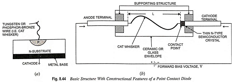
A pointed phosphor-bronze or tungsten wire with a cross-sectional area of a few μm diameter known as a cat whisker, is then pressed against exposed surface of the semiconductor crystal at the opposite side of the base metal. The contact area may be much smaller than the area of cat whisker. An ohmic contact for the cathode terminal of the diode is obtained from the metallic base. A high current pulse of 100-200 mA amplitude and of very short duration (1-100 ms duration), normally obtained from discharging a capacitor, is then passed through the whisker and substrate which results in melting of semiconductor crystal at contact area.
During this process, a number of atoms from the whisker are passed into the crystal which convert the contact area into the P-type semiconductor material. Although the details of forming the rectifying junction cannot be readily understood, but it is believed that a P-N junction with very small contact area is formed at the contact point. The whole assembly is then encapsulated in a ceramic or glass envelope with a suitable supporting structure to provide it mechanical strength [Fig. 8.44 (b)].
A certain amount of bending is maintained in the whisker to sustain the heat expansion due to the power dissipation in the device. The anode terminal of the diode is obtained from the whisker through the supporting structure provided within the envelope. However, a color band is usually provided on the glass envelope for determination of the diode cathode terminal.
The point contact diode provides a very small junction capacitance CT (0.1 to 1 pF) due to its very small area. Further, due to thin P-region with smaller carrier concentration results in smaller storage of minority carriers in the N-type region under forward bias of operation. Thus, the diffusion capacitance CD is also reduced to minimum (negligible in comparison to that of any conventional P-N junction diode). So, the total capacitance of the point contact diode is much smaller than that of any conventional P-N junction diode. Because of very low capacitance, point contact diode is very much suitable for high-frequency applications (of the order of 10 GHz) such as microwave, radio frequency mixers and detector circuits.
Because of small contact area, the point contact diode has lower current ratings than other semiconductor diodes. The lower rating of the diode results in larger value of diode resistance under forward bias of operation. Another important drawback of the point contact diode is that the contact between the whisker and semiconductor is not very rugged and therefore is less reliable than the ordinary P-N junction diodes.
Despite the above mentioned drawbacks, germanium based diodes are widely used in the video detector, envelope detector and detector circuits of radio and television systems.
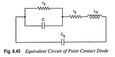
An approximate small-signal equivalent circuit of the point contact diode is shown in Fig. 8.45 where C = CT + CD is the total capacitance of the diode, Cg = ε0A/L is the device geometric capacitance, rd = dV/dI is the nonlinear resistance of the diode and series resistance rs and inductance LS represent the effects of ohmic contacts, bulk semiconductor and whisker.