Tunnel Diode Construction and Working:
Tunnel Diode Construction and Working – The tunnel diode (sometimes called the Esaki diode after its inventor, Dr. Leo Esaki) is a high conductivity, heavily doped two-terminal P-N junction. This diode differs from the normal P-N junction diode in the amount of impurity concentration. The impurity concentration in a normal P-N junction diode is about 1 part in 108, whereas in the tunnel diode the impurity concentration is about 1 part in 103. Because of heavy doping depletion layer width is reduced to an extremely small value of the order of 10-5 mm: reverse breakdown voltage is also reduced to a very small value (approaching zero) resulting in appearance of the diode to be broken for any reverse voltage, and a -ve resistance section is produced in volt-ampere characteristic of the diode. It is found that the reduced depletion layer can result in carriers ‘punching through’ the junction with the velocity of light even when they do not possess enough energy to overcome the potential barrier. The result is that large forward current is produced at relatively low forward voltage (less than 100 mV). Such a mechanism of conduction in which charge carriers (possessing very little energy) punch through a barrier directly instead of climbing over it is called tunneling. That is why such diodes are called the tunnel diodes. Because of heavy doping the tunnel diode can conduct in reverse as well as in forward direction but it is usually used in forward-biased mode.
Construction of Tunnel Diode:
Tunnel Diode Construction are usually fabricated from germanium, gallium arsenide or gallium antimonide. Silicon is not used in the tunnel diode construction, because the ratio of peak value of forward current to the value of valley current (i.e., IP/IV) is maximum in case of gallium arsenide (approximately 20) and comparatively smaller for germanium (roughly 10) but very small in case of silicon (about 3).
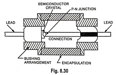
Tunnel diodes are ordinarily manufactured by alloying from gallium arsenide. The source materials are highly doped semiconductor crystals with an impurity concentration of the order of 1025 per cubic metre or more. Tunnel Diode Construction arrangement is shown in Fig. 8.30.
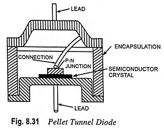
An alternative Tunnel Diode construction arrangement is shown in Fig. 8.31. Such a tunnel diode is called the pellet tunnel diode.
It is to be noted that the tunnel diode, being a low power device, can be easily damaged by heat and static electricity.
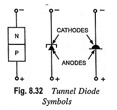
The commonly used schematic symbols for the tunnel diodes are shown in Fig. 8.32.
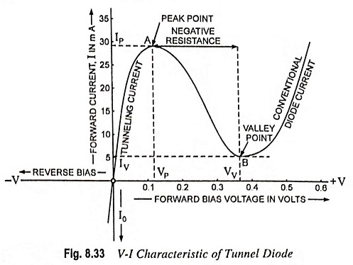
Volt-Ampere Characteristic: Forward V-I characteristic of a tunnel diode is illustrated in Fig. 8.33. Forward bias produces immediate conduction—as soon as forward bias is applied, significant current is produced. The current attains quickly its peak value, IP when the applied forward bias attains a value of VP volts. The current variation in the vicinity of origin is due to quantum mechanical tunneling of electrons through narrow space charge region of the junction. With the further increase in forward voltage, the diode current starts decreasing till it attains its minimum value, called the valley current IV corresponding to valley voltage VV. Thus from peak point A to valley point B the diode current falls with the increase in voltage resulting in negative resistance in this region. In fact this portion AB of the characteristic constitutes the most useful property of the diode. In this region the diode, instead of absorbing power, produces power.
So the tunnel diode can be used as a very high-frequency oscillator. For voltages higher than valley voltage VV current starts increasing as in any normal diode.
Depletion Region and Energy Band Diagrams: The tunneling phenomenon can be explained with the help of energy band diagrams of P- and N-type semiconductor materials.
Because of heavy doping in case of tunnel diode, the depletion region is extremely narrow and, therefore, it does not constitute much of a barrier to the electron flow. As a result, a small forward or reverse bias (not large enough to overcome the barrier potential) can provide charge carriers sufficient energy to cross the depletion region. When this occurs, the charge carriers are said to be tunneling through the barrier.
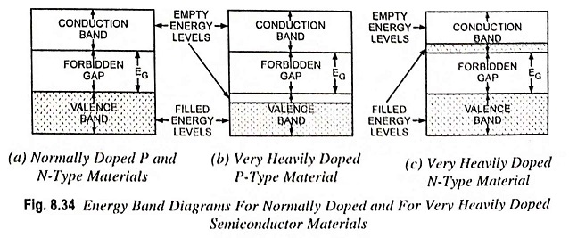
When the semiconductor material is normally doped (either N-type or P-type), electrons fill all the holes in the valence band of energy level and conduction band is empty as illustrated in Fig. 8.34 (a). In case of a heavily doped P-type semiconductor material there is a deficiency of electrons and the valence band cannot be taken as filled. The result is that at the top of valence band there is a layer of empty energy levels, as illustrated in Fig. 8.34 (b). With very heavily doped N-type semiconductor material, there is an abundance of electrons. The result is that; electrons fill the valence band and create a layer of filled energy level at the bottom of the conduction band, as illustrated in Fig. 8.34 (c).
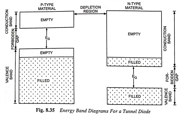
The energy band diagram for a heavily doped unbiased P-N junction is shown in Fig. 8.35. Note that the depletion region is very narrow and the filled levels on the N-side are exactly opposite those on the P-side. In this condition, no tunneling occurs as there are no empty lower energy levels to which electrons from either side might cross the depletion region. It is also to be noted that the conduction and valence bands on P-side are (negatively) higher than those on the N-side. This is due to formation of depletion region and barrier potential as a result of electrons crossing from the N-region to the P-region. The N-region has lost negative charges and P-region has gained them.
When the junction is reverse biased the P-region moves up with respect to the N-region. As a result, filled energy levels on the P-side become opposite empty energy levels on the N-side. At this stage electrons tunnel through the narrow space charge region from the higher energy levels on the P-side to the lower energy levels on the N-side. Despite the fact that the junction is reverse biased, significant current flows. With the increase in reverse bias, more and more electrons tunnel from the P-side to N-side and a larger current flows. Thus the reverse characteristic of a tunnel diode is linear, just like that of a resistor (Fig. 8.33).
When the tunnel diode is forward biased, its initial behavior is similar to that when it is reverse biased. Now, some of the filled energy levels on the N-side shift to a high energy level than empty level on the P-side (Fig. 8.35). Electron tunneling now occurs from the N-side to the P-side. With the increase in forward bias, more and more electrons tunnel from the N-side to the P-side. Eventually, however, a maximum level of tunneling is reached when a band of filled energy levels at the bottom of conduction band on the N-side is directly opposite the band of empty energy levels at the top of the valence band on the P-side. At this stage diode current attains its peak value IP and the forward bias is VP (≈100 mV). With the further increase in forward bias, part of the band of filled energy levels on the N-side is raised to an energy level corresponding to forbidden energy gap on the P-side. Electrons cannot tunnel to a forbidden energy level; thus the current flow due to tunneling is reduced. With continued increase in forward bias, tunneling goes on reducing. When all of the band of filled levels at the bottom of the conduction band on the N-side is raised to a level corresponding to the forbidden energy gap on the P-side, the current flow due to tunneling is reduced to the minimum level, called the valley current IV. Now, however, the normal process of current flow across the forward biased junction begins to take over, as the bias becomes large enough to overcome the barrier potential. For voltages exceeding valley voltage VV, the current starts increasing as in a normal diode
Diode Parameters: We have seen that between IP and IV (points A and B on the V-I characteristic of tunnel diode illustrated in Fig. 8.33) the diode current decreases with the increase in voltage applied across the diode. This region of the characteristic is called the negative resistance region, and the negative resistance RN of the tunnel diode is its most important property. Its value may be determined by computing the slope of the characteristic in the negative resistance region. The value of negative resistance slightly differs from point to point on the negative resistance portion of the characteristic. So RN is usually specified at the centre of the negative resistance region.
Parameters for a typical tunnel diode are given below :
Peak current IP : 1 – 100 mA; Peak voltage VP : 50 – 200 mV; Valley current IV : 0.1 – 5 mA; Valley voltage VV : 350 – 500 mV; Forward bias V : 0.5 – 1 V; Negative resistance RN : – 10 to – 200 Ω.
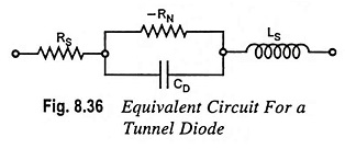
Tunnel Diode Equivalent Circuit: The equivalent circuit for a tunnel diode biased in the negative resistance region is given in Fig. 8.36. RS represents the resistance of the connecting leads to the tunnel diode and the semiconductor material, and is of the order of 5 Ω; LS represents the inductance of the connecting leads and is of the order of 0.5 nH; and CD is junction diffusion capacitance and is of the order of 5 to 100 pF. These factors limit the frequency at which the diode can be operated. Frequency may range from 100 MHz to 10,000 MHz.
Advantages and Disadvantages of Tunnel Diodes:
The advantages of tunnel diodes are low cost, low noise, simplicity, high speed of operation, ease of operation, low power and environmental immunity.
The disadvantages of the tunnel diodes are its low output-voltage swing and being a two-terminal device, it cannot provide isolation between the input and output circuits.
Applications of Tunnel Diode:
The tunnel diode can be used as an amplifier, an oscillator, or a switch. Because of very fast response to inputs, it is almost exclusively a high frequency component. The tunnel diode is, however, not widely used because it is a low current device and also that other better devices are available for the operations listed above.