What is Crossover Distortion and how to eliminate it?
In addition to the distortion introduced due to the nonlinearity of the collector characteristics and due to non-matching of the two transistors, there is one more source of distortion, that is caused by nonlinearity of the input characteristic. Recall that silicon transistors must have at least 0.5 V to 0.6 V of forward base-emitter bias before they will go into conduction. Since in class B push-pull amplifiers the forward bias is produced by the input signal, both of the transistors will be non-conducting (or off), when the input signal is approximately ± 0.5 V. This forms a “dead band” in the input and produces crossover distortion in the output.
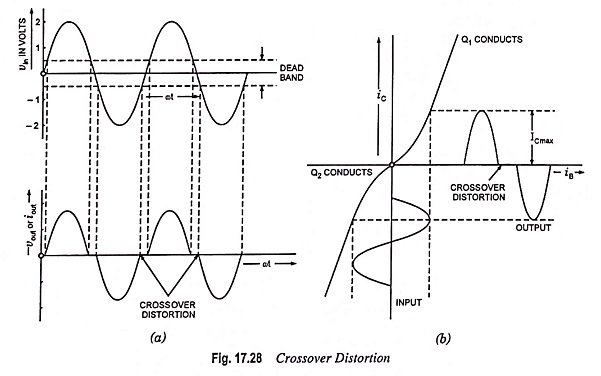
In simple words, crossover distortion occurs as a result of one transistor cutting off before the other begins conducting, as illustrated in Fig. 17.28 (a). The distortion introduced is called the crossover distortion because it occurs during the time operation crossover from one transistor to the other in the push-pull amplifier. The same is shown in Fig. 17.28 (b) by using transfer characteristics of the two transistors.
To eliminate crossover distortion, it is necessary to add a small amount of forward bias to take the transistors to the average of conduction or slightly beyond. This does slightly lowers the efficiency of the circuit and there is a waste of standby power, but it alleviates the crossover distortion problem.
Technically the operation of transistors lies between class B and class A mode. Therefore, the circuit operation is often referred to as being class AB operation.