PN Diode Switching Times:
A P-N junction diode may be used as an electrical switch. The electrical circuit can be made ‘on’ and ‘off’ by forward biasing or reverse biasing the diode. In both the cases, the diode response is accompanied by transient, and an interval of time elapses before the diode recovers to its steady state. The duration of time elapsed before the recovery of the steady state of the diode is called the recovery time, tr. On PN Diode Switching Times from reverse-bias condition to forward-bias condition, the diode takes certain time interval, called the forward recovery time, tfr. The forward recovery time tfr is defined as the time interval between the instant of 10% diode voltage and the instant this voltage attains 90% of its final value. It is found that tfr does not usually constitute a serious practical problem and so only the more important situation of reverse recovery will be discussed here.
Diode Reverse Recovery Time:
As already discussed, when a P-N junction is forward biased a large number of electrons cross over from N-region to P-region and similarly a large number of holes cross over from P-region to N-region. The electrons in the P-type region and the holes in the N-type region establish a large number of minority carriers in each region. The variation of steady-state minority carrier density with distance x from the junction in a forward biased P-N junction is shown in Fig. 7.73 (a). The number of minority carriers is very large. These minority carriers have, in each case, been supplied from the other side of the junction, where, being majority carriers, they are in plentiful supply. The concentration of holes in N-region, Pn is increased above its thermal-equilibrium value Pno. Similarly the concentration of electrons in P-region, np is increased above its thermal-equilibrium value npo. The difference of excess of holes i.e., (Pn – Pno) and excess of electrons i.e., (np – npo) is also shown in the figure.
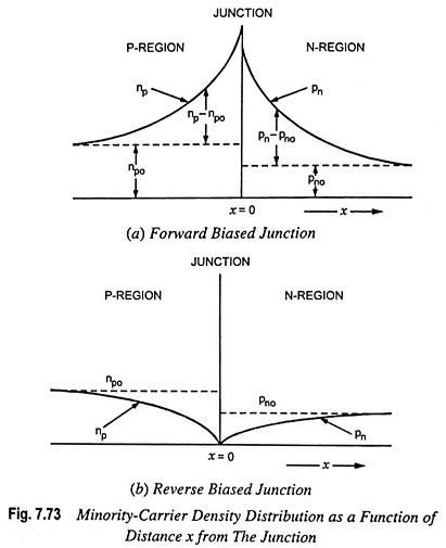
When the junction is reverse biased, the steady-state density of minority carriers is as shown in Fig. 7.73 (b). Far from the junction the minority carriers are equal to their thermal-equilibrium values Pno and npo as is also the situation in Fig. 7.73 (a). As the minority carriers approach the junction, they are rapidly swept across, and the density of minority carriers diminishes to zero at this junction. The reverse saturation current I0 is very small because the density of the thermally generated minority carriers is very small.
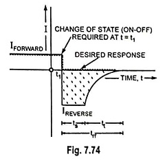
If the external voltage is suddenly reversed in a diode circuit which has been carrying current in the forward direction, the diode current will not immediately fall to its steady-state reverse voltage value, as illustrated in Fig. 7.74. However, because of the large number of minority carriers in both of the regions, the diode current will simply reverse, as illustrated in Fig. 7.74 and stay at this measurable level required for the minority carriers to reduce to the distribution shown in Fig. 7.73 (b) from the minority-carrier distribution shown in Fig. 7.73 (a). The diode will continue to conduct for a time, known as diode reverse recovery time, trr, until excess minority-carrier density Pn – Pno or (np – npo) has dropped normally to zero. In this situation, the current is determined by the external resistance in the diode circuit.
Storage and Transition Times:
The sequence of events occurring on reverse biasing of a conducting diode is shown in Fig. 7.75.
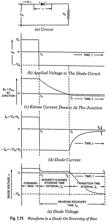
Let the input voltage vin applied to a diode-resistance circuit shown in Fig. 7.75 (a) be reversed abruptly at time instant t1. Up to a time t1, the diode is conducting in forward direction and input voltage vin = VF. Assuming load resistance RL to be large enough to cause voltage drop across it large in comparison with the voltage drop across the diode, the current flowing through the circuit, i ≈ VF/RL ≈ IF. At instant of time t1, the input voltage reverses abruptly to a value -VR. Now the current does not drop to zero, but instead reverses and remains at a value i ≈ -VR/RL ≈ -IR for the time duration ts (storage time interval) required for the minority carriers to return to their majority-carrier state in the opposite region. At instant of time t2, as seen in Fig. 7.75 (c), the injected minority-carrier density at x = 0 has reached the equilibrium state.
Now if we consider the diode voltage v, we find that at time instant t1 the diode voltage falls slightly by (IF+ IR) Rd, where Rd is the diode ohmic resistance, but does not reverse. At time instant t2 the process of sweeping of the excess minority carriers in the vicinity of junction hack has completed. So the diode voltage begins to reverse and the magnitude of diode current begins to decrease. During the time interval t1 to t2, the stored minority charge has remained stored and, therefore, this time interval is called the storage time ts. This is illustrated in Fig. 7.75 (e).
After all excess minority carriers are swept out or recombined in the neighborhood of junction, the diode voltage begins to reverse and the magnitude of diode current begins to fall exponentially to the normally steady-state reverse saturation current value. The time duration which elapses between t2 and the time instant t3 when the diode has nominally recovered, is called the transition time tt. This recovery time interval will be completed when the minority carriers, which are at some distance from the junction, have diffused to the junction and crossed it and when, in addition, the junction transition capacitance across the reverse-biased junction has charged through load resistance RL to the voltage -VR.
The sum of the storage time ts and transition time tt is called the diode reverse recovery time trr i.e., ts + tt = trr.
Manufacturers normally specify the reverse recovery time of a diode trr in a typical operating condition in terms of the current waveform of Fig. 7.75 (d). The time trr is the interval from the current reversal at t = t1 until the diode has recovered to a specified extent in terms either of the diode current or of the diode resistance.
Naturally trr is an important consideration in high speed PN Diode Switching Times applications. Most commercially available PN Diode Switching Times have reverse recovery time trr in the range of a few nanoseconds to 1 μs. Units are available, however, with a trr of only a few hundred picoseconds.