Transistor Switching Times:
For Transistor Switching Times, the switching speed of the device can be an important quantity. Consider the circuit in Fig. 8-18(a). When the base input current is applied, the transistor does not switch on immediately. Like frequency response, the Transistor Switching Times is affected by junction capacitance and the transit time of electrons across the junctions. The time between the application of the input pulse and commencement of collector current flow is termed the delay time (td), [see Fig. 8-18(b)]. Even when the transistor begins to switch on, a finite time elapses before IC reaches its maximum level. This is known as the rise time (tr). The rise time is specified as the time required for IC to go from 10% to 90% of its maximum level. As illustrated, the turn-on time (ton), is the sum of td and tr.
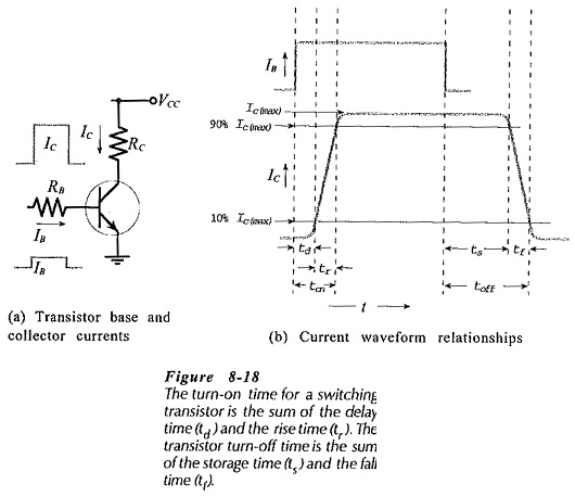
When the input current is switched off, IC does not go to zero until after a turn-off time toff, made up of a storage time (ts), and a fall time (tf), as illustrated. The fall time is specified as the time required for IC to go from 90% to 10% of its maximum level. The storage time is the result of charge carriers being trapped in the depletion region when a junction polarity is reversed.
When a transistor is in a saturated on condition, both the collector-base and emitter-base junctions are forward biased. At switch-off both junctions are reverse biased, and before IC begins to fall, the stored charge carriers must be withdrawn or made to recombine with opposite-type charge carriers.
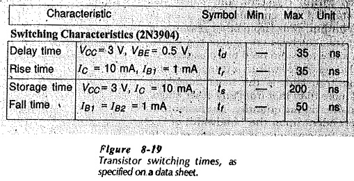
For a fast-switching transistor, ton and toff must be of the order of nanoseconds. The 2N3904 transistor data sheet portion in Fig. 8-19 specifies the following Transistor Switching Times: td = 35 ns, tr = 35 ns, ts = 200 ns, and tf = 50 ns.