IC Controller for Switching Regulators:
The functional block diagram of a MC34063 integrated circuit controller is shown in Fig. 17-38. This IC is designed to be used as a variable off time IC Controller for Switching Regulators.
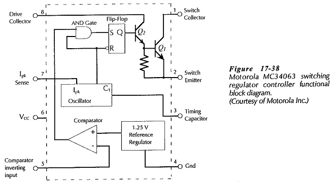
The components parts of the diagram in Fig. 17-38 are:
- Switching transistor (Q1) controlled by transistor Q2.
- Set-reset flip-flop with input terminals S and R, and output Q.
- AND gate that controls Q1 and Q2 by controlling the flip-flop.
- Oscillator that generates a square wave output at the desired switching frequency. The oscillator frequency is set by an externally-connected timing capacitor (CT) at terminal 3.
- Current limiter terminal (Ipk sense). This input to the oscillator permits Q1 to be turned off via the reset terminal of the flip-flop.
- Comparator for comparing the output and reference voltages.
- Reference voltage source (1.25 V).
Step-Down Converter Using an MC34063:
Figure 17-39 shows an MC34063 connected to function as a step-down converter. The positive terminal of the supply is connected to terminal 6, and the negative (grounded) terminal is connected to terminal 4. Note that a 100 μF capacitor (C2) is connected from terminal 6 to ground (right at the IC terminals) to smoothe supply-line pulses that result from fast load current changes.
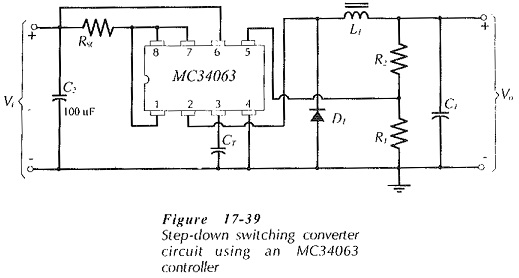
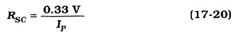
The supply voltage (Vi) is connected (via RSC) to the collectors of Q1 and Q2 at terminals 8 and 1, (see Fig. 17-38). Resistor RSC (connected to terminal 7) senses the peak supply current (IS) and provides a voltage drop to turn Q1 off when the current exceeds the maximum design level. The equation for the current-limiting resistor is given on the device data sheet as,
The output voltage (Vo) is divided across resistors R1 and R2 and applied to the inverting input of the voltage comparator to compare it to the reference voltage (Vref). The voltage across R1 must be equal to the Vref when the circuit is operating correctly, and the voltage across (R1 + R2) equals Vo. As in all voltage divider designs, the resistor current should be much larger than the device input bias current; the comparator input current in this case.
The timing capacitor (CT), connected from terminal 3 to ground, is selected for the desired on time of the switching transistor. An equation for the capacitance of CT is given on the IC data sheet;
![]()
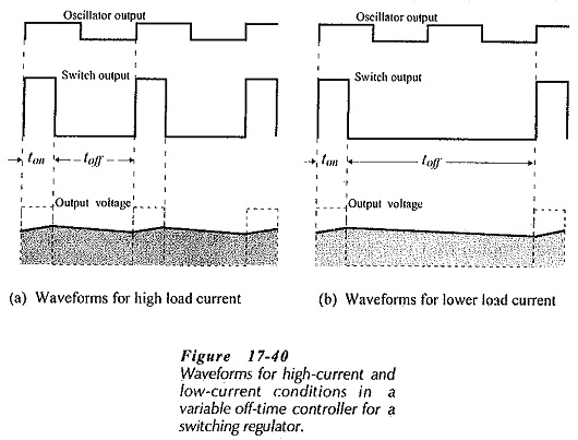
Variable Off Time Modulator:
Switching converter circuits are designed to supply a particular maximum load current. For a converter circuit using an MC34063 controller, the circuit waveforms are typically as shown in Fig. 17-40(a) when supplying full load current. Transistor Q1 (in Fig. 17-38) is switched on at the start of the each cycle of the oscillator square wave output. Also, ton and toff add up to the time period (T) of the oscillator, as illustrated. When the load current is low, capacitor C1 discharges more slowly than when supplying full load current, [see Fig. 17-40(b)]. So, VR1 (in Fig. 17-39) has not dropped below Vref by the beginning of the next cycle of the oscillator square wave. Consequently, Q1 is not switched on again at this point, and so the pulse waveform frequency at Q1 emitter is now lower than the oscillator frequency. A switching converter controller designed to operate in this way is known as a variable off-time modulator.
Catch Diode Selection:
The diode power dissipation can be calculated approximately from the output current and the diode voltage drop;
![]()
The reverse recovery time (trr) of the diode should be less than one tenth of the minimum diode on or off time, which ever is smaller;
![]()
Diode Snubber:
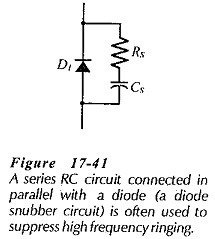
A diode snubber is a series RC circuit connected across the catch diode to suppress high frequency ringing that can be produced by resonance of the inductance and capacitance of components and connecting leads. (Termed parasitic inductance and capacitance.) A diode snubber circuit is shown in Fig. 17-41. The capacitance of CS is usually selected in the range of four to ten times the diode junction capacitance (CD), and then the resistance of RS is calculated from CS and the ringing frequency (fr).
High Power Converters:
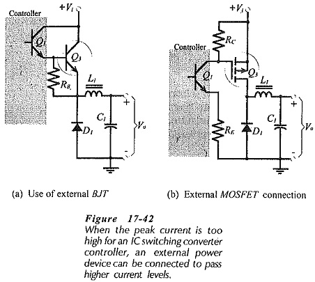
When the load current of a IC Controller for Switching Regulators is too high for the controller internal transistor, an externally-connected device can be employed. Figure 17-42(a) illustrates how a high-power BJT (Q3) should be connected for use with a step-down converter, and Fig. 17-42(b) shows how an external FET should be connected. Resistor RB at the base of Q3 in Fig. 17-42(a) ensures that Q3 is biased off when Q1 switches off. For the p-channel MOSFET (Q3) in Fig. 17-43(b), resistors RC and RE are selected to give a gate-channel voltage (VRC) that will switch Q3 on when Q1 is on.