8288 Bus Controller:
Figure 5.37 shows the 8288 bus controller which is used in the maximum-mode operation of 8086 CPU. This IC receives four inputs such as S̅2, S̅1, S̅0 status signals and CLK from 8086. There are two sets of output command signals.
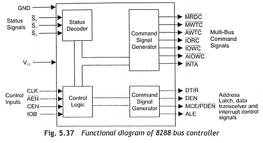
The first set of output command signals are the MULTIBUS command signals. These are the conventional M̅E̅M̅R̅, M̅E̅M̅W̅, I̅O̅R̅ and I̅O̅W̅ control signals. These signals are renamed as M̅R̅D̅C̅, M̅W̅T̅C̅, I̅O̅R̅C̅ and I̅O̅W̅C̅ respectively. Here, C stands for command. A̅M̅W̅C̅ and A̅I̅O̅W̅C̅ are advanced memory and I/O write commands. These outputs are enabled one clock cycle earlier than the normal write commands. Some memory and I/O devices require this wider write pulse width.
The second set of output signals of the 8288 Bus Controller are the bus control signals DT/R̅, D̅E̅N̅, ALE and MCE/P̅D̅E̅N̅. MCE/P̅D̅E̅N̅ is an output signal which has two functions depending on the 8288’s mode of operation such as I/O bus control or system bus control.
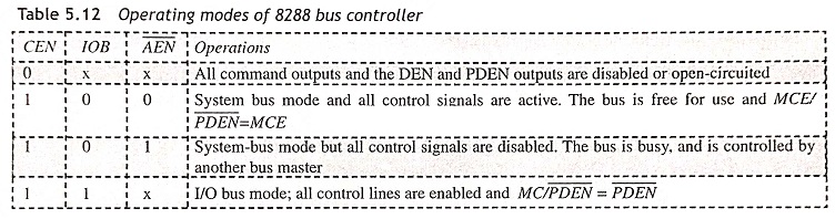
The three 8288 control inputs CEN, IOB and A̅E̅N̅ determine the operating mode as given in Table 5.12. When CEN and IOB are high or of logic level 1, the 8288 operates in the I/O bus mode and the MCE/P̅D̅E̅N̅ output acts as a peripheral data enable. The function of MCE/P̅D̅E̅N̅ is identical to DEN but it is active only during I/O instructions. This allows the 8288 to control two sets of buses such as the normal system buses and a special I/O bus dedicated to the processor.
During the system-bus mode, the control signals are active only while the address enable signal A̅E̅N̅ and IOB inputs are low. In this mode of operation, several 8288s IC and 8086 processors can be interfaced to the same set of bus lines. The bus mediator selects the active processor after enabling only one 8288 bus controller through an A̅E̅N̅ signal. The MCE/P̅D̅E̅N̅ signal becomes MCE (Master Cascade Enable). In this mode, the MCE/P̅D̅E̅N̅ signal is used to read the address from a master priority interrupt controller, PIC.
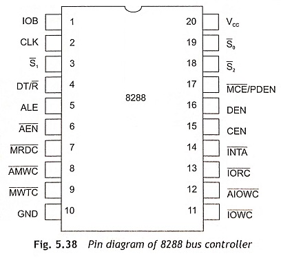
The pin diagram of the 8288 bus controller is shown in Fig. 5.38. The functions of the pins are described in this section.
S̅2, S̅1, S̅0 (Status Input Signals) These arc bus cycle status signals. These are decoded and control signals are generated.
CLK This is an input signal. It is connected to CLK output of the clock generator 8284.
A̅E̅N̅, CEN, IOB These are bus priority and mode control signals. A̅E̅N̅ (bus priority control/enable), CEN(Command Enable) and IOB (mode control) signals are used to generate various control signals.
M̅R̅D̅C̅ (Memory Read Control Signals) These command signals are used to load the content of memory location on the data bus.
M̅W̅T̅C̅ (Memory Write Control Signals) These command signals are used to store the available data on the data bus to the specified memory location.
I̅O̅R̅C̅ (I/O Read Control Signals) The I/O device is able to put the available data of the addressed port on the data bus.
I̅O̅W̅C̅ (I/O Write Control Signals) The I/O device is able to accept the available data port on the data bus and send to the addressed port.
A̅M̅W̅C̅ (Advance Memory Write Control Signal) This signal is activated one clock period earlier than M̅W̅T̅C̅.
A̅I̅O̅W̅C̅ This signal is activated one clock period earlier than I̅O̅W̅C̅.
MCE/P̅D̅E̅N̅ Cascade/Peripheral data Enable. This signal is used in Priority Interrupt Controller 8259A.
I̅N̅T̅A̅ (Interrupt Acknowledge) This is used as output signal during two interrupt acknowledge bus cycles and is used as memory read control signal.
ALE Address Latch Enable signal.
DT/R̅ Data Direction Control signal.
DEN Data buffer control signal.
VCC Power Supply Input + 5 V.
GND (Ground) This pin is connected system ground.