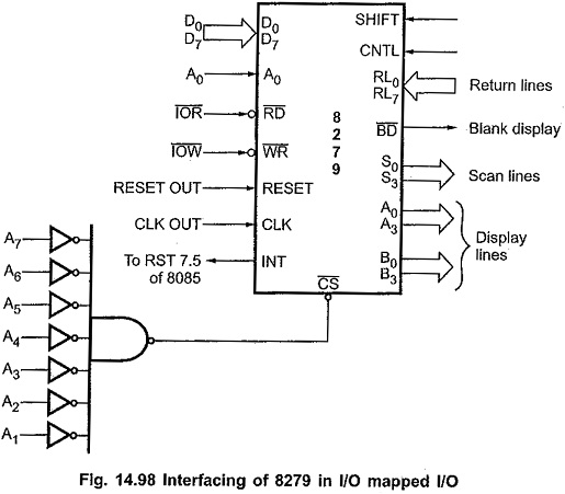
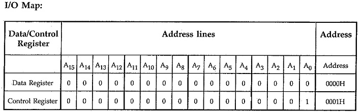
8279 Keyboard Display Controller Interfacing with 8085:
Fig. 14.98 shows the 8279 Keyboard Display Controller Interfacing with 8085 in I/O mapped I/O technique. Here RD and WR signals are activated when IO/M signal is high, indicating I/O bus cycle. Reset out signal from 8085 is connected to the Reset signal of the 8279. CLK input of 8279 is driven from the clock out of 8085. A0 signal from the 8085 is connected to the A0 input of 8279. The chip select signal, CS is generated using decoding circuit. Interrupt signal from the 8279 is connected to the RST 7.5 input of the 8085. It can also be connected to the RST 5.5, RST 6.5 or Trap input of 8085.

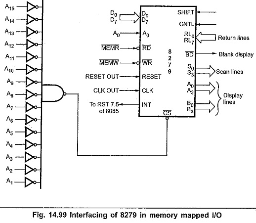
Interfacing 8279 with 8085 in memory mapped I/O:
Fig. 14.99 shows the 8279 Keyboard Display Controller Interfacing with 8085 in memory mapped I/O technique. Here, RD and WR signals are activated when IO/M signal is low, indicating memory bus cycle. To get absolute address, all remaining address lines (A1-A15) are used to decode the address for 8279. Other signal connections are same as in I/O mapped I/O.
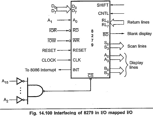
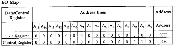
Interfacing 8279 with 8086 in I/O Mapped I/O:
Fig. 14.100 shows the interfacing of 8279 with 8086 in I/O mapped I/O technique. Here RD and WR signals are activated when M/IO signal is low, indicating I/O bus cycle. Reset out signal from 8086 system is connected to the Reset signal of the 8279. CLK input of 8279 is driven from the clock signal of 8086 system. A1 signal from the 8086 is connected to the A0 input of 8279. The chip select signal, CS is generated using decoding circuit. Interrupt signal from the 8279 is connected to the interrupt input of 8086.
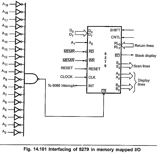
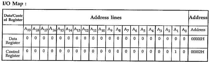
Interfacing 8279 with 8086 in Memory Mapped I/0:
Fig. 14.101 shows the interfacing of 8279. with 8086 in memory mapped,I/O technique. Here, RD and WR signals are activated when M/IO signal is high, indicating memory bus, cycle. To get absolute address, all remaining address lines (A2-A19) are used to decode the address for 8279. Other signal connections are same as in I/O mapped I/O.