Memory Interfacing in 8085:
Memory is an integral part of a microprocessor system, and in this section, we will discuss how to interface a memory device with the microprocessor. The Memory Interfacing in 8085 is used to access memory quite frequently to read instruction codes and data stored in memory. This read/write operations are monitored by control signals. The microprocessor activates these signals when it wants to read from and write into memory. In the last section we have already seen the memory read and memory write machine cycles, and status of the RD, WR and IO/M status signals for read/write operation. In the following section we will see memory structure and its requirements, concepts in Memory Interfacing in 8085 and interfacing examples.
Memory Structure and its Requirements:
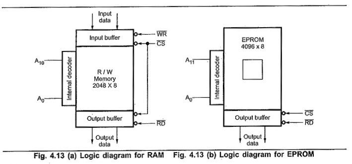
As mentioned earlier, read/write memories consist of an array of registers, in which each register has unique address. The size of the memory is N x M as shown in Fig. 4.13 (a) where N is the number of registers and M is the word length, in number of bits.
Basic Concepts in Memory Interfacing:
For Memory Interfacing in 8085, following important points are to be kept in mind.
- Microprocessor 8085 can access 64Kbytes memory since address bus is 16-bit. But it is not always necessary to use full 64Kbytes address space. The total memory size depends upon the application.
- Generally EPROM (or EPROMs) is used as a program memory and RAM (or RAMs) as a data memory. When both, EPROM and RAM are used, the total address space 64Kbytes is shared by them.
- The capacity of program memory and data memory depends on the application.
- It is not always necessary to select 1 EPROM and 1 RAM. We can have multiple EPROMs and multiple RAMs as per the requirement of application.
- We can place EPROM/RAM anywhere in full 64 Kbytes address space. But program memory (EPROM) should be located from address 0000H since reset address of 8085 microprocessor is 0000H.
- It is not always necessary to locate EPROM and RAM in consecutive memory For example : If the mapping of EPROM is from 0000H to OFFFH, it is not must to locate RAM from 1000H. We can locate it anywhere between 1000H and FFFFH. Where to locate memory component totally depends on the application.
The memory interfacing requires to :
- Select the chip
- Identify the register
- Enable the appropriate buffer.
Microprocessor system includes memory devices and I/O devices. It is important to note that microprocessor can communicate (read/write) with only one device at a time, since the data, address and control buses are common for all the devices. In order to communicate with memory or I/O devices, it is necessary to decode the address from the microprocessor. Due to this each device (memory or I/O) can be accessed independently. The following section describes common address decoding techniques.
Address Decoding Techniques :
- Absolute decoding/Full Decoding
- Linear decoding/Partial Decoding
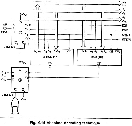
Absolute decoding/Full Decoding:
In absolute decoding technique, all the higher address lines are decoded to select the memory chip, and the memory chip is selected only for the specified logic levels on these high-order address lines; no other logic levels can select the chip. Fig. 4.14 shows the Memory Interfacing in 8085 with absolute decoding. This addressing technique is normally used in large memory systems.
Linear decoding/Partial Decoding:
In small systems, hardware for the decoding logic can be eliminated by using individual high-order address lines to select memory chips. This is referred to as linear decoding. Fig. 4.15 shows the addressing of RAM with linear decoding technique. This technique is also called partial decoding. It reduces the cost of decoding circuit, but it has a drawback of multiple addresses (shadow addresses).
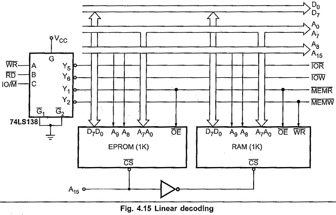
Fig. 4.15 shows the addressing of RAM with linear decoding technique. A15 address line, is directly connected to the chip select signal of EPROM and after inversion it is connected to the chip select signal of the RAM. Therefore, when the status of A15 line is ‘zero’, EPROM gets selected and when the status of A15 line is ‘one’ RAM gets selected. The status of the other address lines is not considered, since those address lines are not used for generation of chip select signals.
Wait State Generator:
We have seen that wait states can be introduced in the machine cycles using READY signal to interface slower memory devices. In this section we are going to see the circuits for wait state generator and applications of those circuits to interface slower memories.
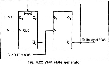
The Fig. 4.22 shows the circuit for wait state generator. This circuit generates single wait state in every machine cycle. The circuit operation is given below.
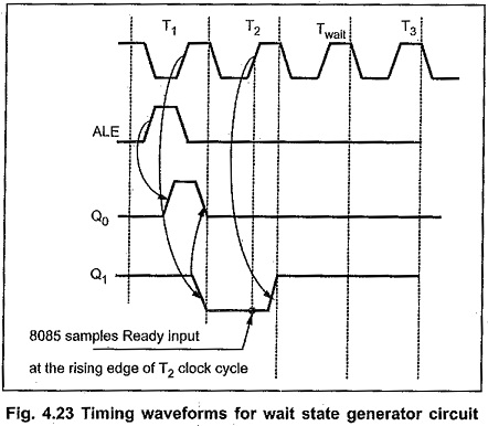
In T1, the ALE signal is activated, which makes output Q0 of the first D flip-flop high, assuming RESET (R) is one. In the next clock pulse i.e. in the next low to high transition of CLKOUT signal of the 8085, the output Q1 of the second D flip-flop goes low. The low on the Q1 output initiates 8085 to enter wait state and resets the first D flip-flop making its Q0 output low, since Q1 is connected to the ready input of 8085 and to the reset input of the first D flip-flop. At next low to high transition of CLKOUT, Q of the second D flip-flop goes high making READY pin high and inactivating reset input of the first flip-flop. Fig. 4.23 shows the timing waveforms for this circuit.
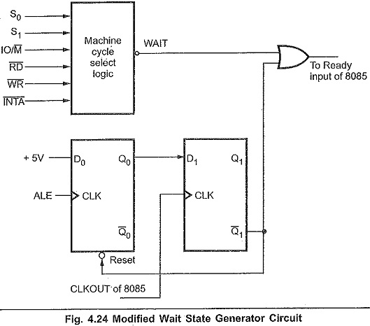
This circuit can be modified to introduce wait states for a particular machine cycle. The modified circuit of wait state generator is shown in Fig. 4.24. The modified circuit will generate a single WAIT state for any machine cycle for which the WAIT output of the machine cycle select circuit is logic 0.