8096 Memory Space:
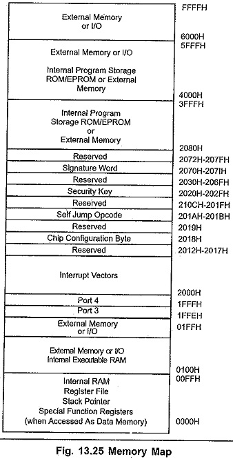
The addressable memory space on the 8096 Memory Space consists of 64 K bytes, most of which is available to the user for program or data memory. Locations which have special purposes are 0000H through 00FFH and 1FFEH through 2080H. All other locations can be used for either program or data storage or for memory mapped peripherals. A memory map is shown in Fig. 13.25.
Reserved Memory Spaces:
Locations 1FFEH and 1FFFH are reserved for Ports 3 and 4 respectively. This is to allow easy reconstruction of these ports if external memory is used in the system. If ports 3 and 4 are not going to be reconstructed then these locations can be treated as any other external memory location.
The 9 interrupt vectors are stored in locations 2000H through 2011H. The 9th vector is used by intel development systems. Internal locations 2012H through 207FH are reserved for Intel’s factory test code. To ensure compatibility with future parts external locations 2012H through 207FH must contain the hex value FFH.
Resetting the 8096 Memory Space causes instructions to be fetched starting from location 2080H. This location was chosen to allow a system to have up to 8K of RAM continuous with the register file.
System Bus:
External memory is addressed through lines AD0 through AD15 which form a 16-bit muliplexed (address/data) data bus. These lines share pins with I/O ports 3 and 4. The external latch (74LS373) is used to demultiplex the bus at the falling edge of the Address Latch Enable (ALE) signal . To avoid confusion during the explanation of the memory system it is reasonable to give names to the demultiplexed address/data signals. The address signals will be called MA0 through MA15 (Memory Address), and the data signals will be called MD0 through MD15 (Memory Data).
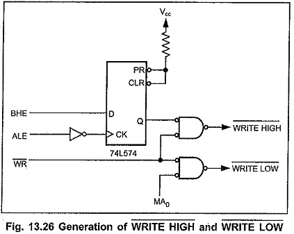
Since the 8096’s external memory can be addressed as either bytes or words, the decoding is controlled with two signals: Bus High Enable (BHE) and Address Data Line 0 (AD0). The BHE line must be latched, as shown in the Fig. 13.26. When BHE is active (low), the memory connected to the high byte of the data bus should be selected. When MA0 is low the memory connected to the low byte of the data bus should be selected. Accesses to a 16-bit wide memory can be made as shown in Table 13.8.
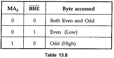
When a memory block is being used only for reads, BHE and. MA0 need not be decoded.
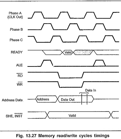
Fig. 13.27 shows the memory read/write cycles. When an external memory fetch begins, the address latch enable (ALE) line goes high, the address is put on AD0 -AD15 and BITE is set to the required state ALE then goes low, the address is taken off the pins, and the RD (Read) signal goes low. The READY line can be pulled low to hold the processor in this condition for a few extra state times. The READY line is usually used to hold the processor in the above condition in order to allow access to slow• memories or for DMA purposes.